The post Top Automotive OEMs Collaborate for Faster ADAS Improvement appeared first on Counterpoint.
]]>Ahead of NVIDIA’s GTC event next week, we are re-sharing parts of our Accelerating Automotive Intelligence: Car OEMs Forge Strategic Alliances with ADAS SoC Providers, 2023 Update report, which outlines how key vendors like NVIDIA – as well as a host of others – are working in partnership with the OEMs. Sharing resources and knowledge is helping the industry to move faster in advancing ADAS and autonomous driving.
Key points from the report
The major OEM and autonomous SoC supplier alliances are those with chipmakers NVIDIA, Qualcomm, Mobileye while smaller providers jockey for position.
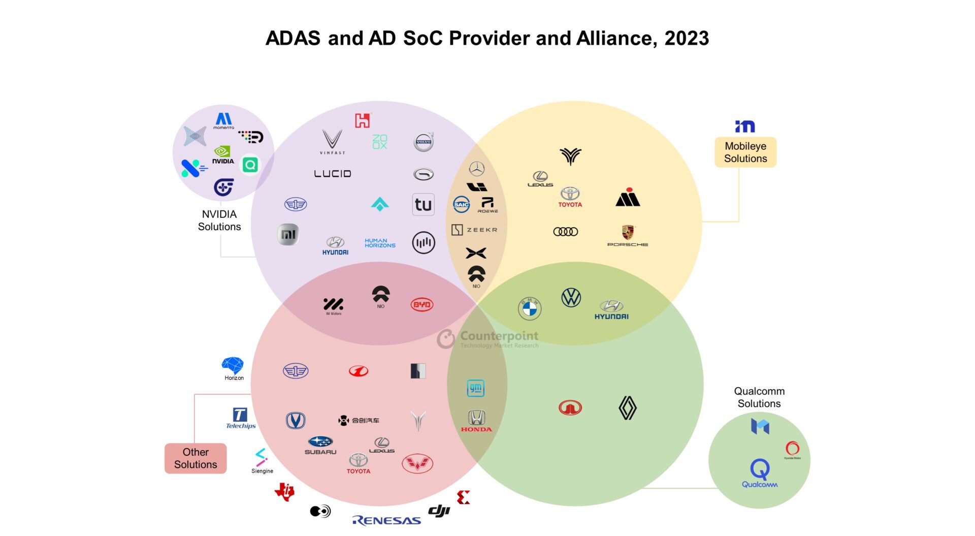
NVIDIA’s involvement in ADAS and AD chip technology has been significant in recent years with the company advancing in developing powerful and efficient chips tailored for these applications. Among its key partners are Volvo for autonomous driving, SAIC for intelligent EVs, BYD for next-gen ADAS as well as a host of others.
Qualcomm’s robust roadmap is facilitating collaboration with the likes of Renault to develop centralized compute architecture of the OEMs next-gen SDVs. It’s also working with GM on next-gen ADAS and GWM for autonomous driving in upcoming models.
Mobileye was one of the early movers, establishing early collaborations with Chinese EV OEMS to provide ADAS chips; the company’s closed ecosystem and relatively lower computing power has resulted in those companies transitioning to alternative solutions.
But Mobileye remains a key player, working together with the likes of Porsche and Volkswagen to develop ADAS and AD tech as well as autonomous driving systems.
Other major providers include Renesas which works closely with compatriot Honda, and German giant Continental which jointly announced a strategic partnership with Ambarella to develop full-stack hardware and software solutions for assisted and automated driving systems.
Our 18 page report has the full list of key ADAS AP-SoC providers and partnerships and is available for clients here.
Related Posts
The post Top Automotive OEMs Collaborate for Faster ADAS Improvement appeared first on Counterpoint.
]]>The post Arm-based PCs to Nearly Double Market Share by 2027 appeared first on Counterpoint.
]]>Personal computers (PCs) based on Arm architecture will grow in popularity and their market share will almost double from 14% now to 25% by 2027, according to Counterpoint Research’s latest projections. The ability of Arm-based hardware to run Mac OS has allowed Apple to capture 90% of the Arm-based notebook computer market. However, the full support of Windows and Office365 and the speed of native Arm-based app adoption are also critical factors in determining the Arm SoC penetration rate in PCs. Once these factors are addressed, Arm-based PCs will become a viable option for both daily users and businesses.
As more existing PC OEMs/ODMs and smartphone manufacturers enter the market, they will bring their expertise in Arm-based hardware and software, which will further boost the popularity of Arm-based PCs. The availability of more native Arm-based apps will also increase user comfort and familiarity with the platform. Overall, the trend towards Arm-based PCs is expected to continue and their market share will likely increase significantly in the coming years.
Notebook Shipment Share by CPU/SoC Type
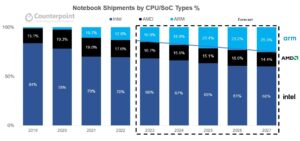
Source: Counterpoint Global PC Forecast, Q4 2022
Arm-based PC SoCs to compete with x86 CPUs
- Arm-based PC SoCs are highly customizable. Unlike x86 CPUs, which are designed to be general-purpose processors, Arm-based SoCs can be tailored to specific use cases. This means that SoCs can be designed with a greater number of high-performance CPU cores and highly integrated memory, enabling them to compete with x86 CPUs. Their custom cores can enable more advanced features that are not possible with off-the-shelf processor cores, and allow for better integration with hardware and the operating system. Furthermore, Arm-based SoCs can incorporate highly integrated memory, resulting in faster and more efficient memory access. This can lead to improved performance in graphics-intensive tasks by enabling faster data access and sharing between the CPU and GPU.
- Arm-based SoCs offer several advantages over x86 CPUs, including lower power consumption and improved thermal efficiency. Additionally, their integrated AI-feature cores make them superior to x86 CPUs. They are designed with power efficiency in mind and can be customized to meet specific power requirements. This makes them ideal for use in mobile devices and laptops, where battery life is crucial. With the increasing demand for AI capabilities, there is a growing need to enhance various multimedia tasks, such as image and video encoding and compression, noise cancellation, vocal enhancement, and style transfer. By integrating AI technology into Arm-based notebooks, these tasks can be performed more efficiently, resulting in improved performance and user experience. Moreover, the integration of GPUs can further enhance the device’s overall performance by accelerating computational tasks such as machine learning and image recognition. This allows for faster and more accurate results, making it possible to run more advanced applications and software on Arm-based devices.
Arm-based PCs integrate more components into compact devices, allow multiple form factors
- The size and weight of PCs are expected to decrease with the introduction of Arm-based SoCs. This will result in a smaller size difference between Arm-based PCs and tablets, facilitating easier integration of these two form factors by manufacturers. This is likely to lead to an increase in the production of laptop-tablet hybrids that can seamlessly switch between the two modes. With the growing popularity and affordability of these devices, convergence between laptop and tablet form factors is likely to intensify.
Arm-based PC Potential Applications

Source: Counterpoint Research, Q1 2023
- ‘Windows on a Stick’ or ‘Windows To Go’ is a portable version of Windows that runs from a USB flash drive and can be used on any compatible x86 PC. Small form-factor devices like this face hardware resource limitations, but Arm-based SoCs offer better performance and integration. This makes them especially useful for small devices like the OS on Stick, providing better performance and more efficient use of space.
- The SoCs being used in VR headsets currently are typically based on smartphone-grade processors, which are designed to balance performance and power efficiency for use in mobile devices. While these SoCs can provide good performance for VR applications, they may not be able to match the performance of high-end PC-based processors in more demanding use cases. However, if Arm-based PC-grade SoCs were used in VR headsets instead, they could allow VR headsets to provide PC-like performance, with the ability to handle more complex and demanding VR applications. In addition to the improved performance, using Arm-based PC-grade SoCs in VR headsets could also enable the use of PC-like applications and provide users with access to a wider range of software and applications, as well as more familiar user interfaces and tools.
Conclusion
Arm-based PC SoCs offer several advantages over x86 CPUs, including customizability, lower power consumption, and integrated AI and GPUs. The rise of Arm-based PCs is expected to continue with the support of Windows and Office365, native apps, and industry experts. This trend is likely to lead to the integration of laptop and tablet form factors and the use of Arm-based SoCs in small devices and VR headsets.
Related Blogs/PRs:
- PlayStation VR2 Review: Great Experience But Tough Competition in Store, MARCH 16, 2023, BY BRADY WANG
- Arm Laptops to Remain Resilient Amid Global PC Market Weakness, FEBRUARY 8, 2023, BY WILLIAM LI
- Global PC Shipments See Record YoY Decline in Q4 2022, JANUARY 19, 2023, BY WILLIAM LI
- VR Headset See-through Tech to Help in MR Development, DECEMBER 20, 2022, BY BRADY WANG
- Global PC Shipments’ Double-digit Crash in Q3, OCTOBER 25, 2022, BY WILLIAM LI
- M1 Pro, M1 Max Give Definitive Push to Apple’s M1 Journey, OCTOBER 25, 2021, BY BRADY WANG
Related Reports:
- Global Quarterly Arm PC forecast Q4 2022, Mar 9, 2023, Author : WILLIAM LI
- Global Quarterly Arm PC tracker Q4 2022, Mar 9, 2023, Author : WILLIAM LI
- Apple M1 Macs Review, May 6, 2021, Author : BRADY WANG
The post Arm-based PCs to Nearly Double Market Share by 2027 appeared first on Counterpoint.
]]>The post PlayStation VR2 Review: Great Experience But Tough Competition in Store appeared first on Counterpoint.
]]>Sony’s new PlayStation VR2 (PSVR2) is a tethered VR headset designed for its PlayStation 5 (PS5) gaming console. The headset aims to provide immersive and realistic VR gaming experiences on the PS5. It has a single cable connection to the console and a built-in camera for tracking. It also comes with two sense controllers that have adaptive triggers and haptic feedback. The PSVR2 has an OLED display with a resolution of 2000×2040 per eye, refresh rate of up to 120Hz and a field of view of 110 degrees.
PSVR2’s features and advantages: Enhanced VR gaming experience
- The PSVR2 incorporates foveated rendering, which leverages eye-tracking to render only those areas of the screen that the user is directly looking at, resulting in less detailed peripheral vision. This approach can significantly enhance performance, reduce computing power usage from the SoC, and decrease system costs. As a result, this technology is expected to become a standard feature in future VR headsets.
- The PSVR2 delivers an even more engaging and true-to-life gaming experience compared to its predecessor. This is made possible by its advanced OLED display that boasts a higher resolution and wider field of view (FOV), along with a faster refresh rate that minimizes motion sickness and blur.
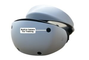 The PSVR2’s built-in cameras eliminate the hassle of external sensors and cables. Furthermore, the controllers of the PSVR2 come equipped with haptic feedback and vibration that realistically simulate tactile sensations.
- The PSVR2 still employs a wired connection, but the cable has been designed to help reduce the weight of the headset and improve comfort during use. This approach can also bring cost savings and enable the PS5 chip to be fully utilized, unlike most all-in-one VR headsets that may have to sacrifice image quality to prevent overheating and reduce power consumption.
PSVR2 falls behind next-gen VR headsets in key areas
- The PSVR2 may not be able to compete with the performance and features of next-generation VR headsets, which offer higher resolution, wider field of view, eye-tracking and wireless streaming.
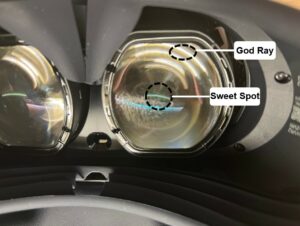
- The PSVR2 is equipped with an OLED display paired with Fresnel lenses, which can cause various discomforts such as smaller sweet spots (aka eye box) and “god rays”. The sweet spots in a VR headset are the ideal position to get the best visual quality by keeping the eyes directly behind the center of the lenses.
- The PSVR2’s OLED display is not immune to the Mura effect, which is a common issue in OLED displays but could be fixed by calibration and compensation techniques. The Mura effect causes irregularities in brightness and color across the screen, resulting in an uneven appearance, particularly in darker scenes.
- In contrast to the Quest Pro or Pico4, which have integrated color cameras to enable the color video see-through (VST) functionality, the PSVR2’s black-and-white VST is limited to the use for safety, preventing its application in other areas, such as MR applications, with greater potential for interaction within the surrounding physical environment. This limitation may impact the system’s ability to offer more immersive experiences.
A pricey VR experience with limited game library and compatibility
- The PSVR2 may not have enough original or exclusive games to justify its price and investment, especially for gamers who are looking for a diverse and immersive VR experience.
- The PSVR2 is not backward compatible with PSVR games, meaning that it cannot play the existing library of VR games for the PlayStation 4. However, some PSVR games will receive PSVR2 ports or free upgrades.
- The PSVR2 comes with a hefty price tag of $549, which may discourage some prospective buyers who have already paid $499 for the PS5 console. Besides, the PSVR2 requires a PS5 console to function, which restricts its compatibility and availability compared to standalone or PC-based VR headsets.
- The PSVR2 presents exceptional and thrilling possibilities for VR gaming enthusiasts. With its exclusive games like Horizon: Call of the Mountain, Resident Evil 8 and Gran Turismo 712, the PSVR2 showcases its abilities and appeals to PlayStation fans. In addition, the PSVR2 boasts innovative features such as haptic feedback, adaptive triggers and headset rumble, which greatly enhances the immersion and interactivity of VR gaming.
- SONY’s decision to only allow the PSVR2 to connect with the PS5 has indirectly reduced the potential for the headset’s sales. Besides, the PSVR2 is unable to access other VR resources, such as VR movies or the vast library of games available on Steam, via a PC or other consoles.
Conclusion
The PSVR2 attempts to strike a delicate balance between cost-effectiveness and exceptional performance, boasting advanced features like foveated rendering and haptic feedback, as well as a higher resolution OLED display and wider field of view. It does encounter challenges and limitations, such as its steep price point and inability to run PC VR games and applications. The headset may also signal the end of an era for staunch supporters of tethered VR headsets. Ultimately, while the PSVR2 is able to extend the lifespan of VR on the PlayStation console, it falls short of branching out into new markets or unlocking the potential for additional VR applications in the future.
For more information, please refer to our forthcoming evaluation report on the PSVR2.
Related Posts
The post PlayStation VR2 Review: Great Experience But Tough Competition in Store appeared first on Counterpoint.
]]>The post AI Voice Assistants to Push Success of Autonomous Driving, Software-defined Vehicle appeared first on Counterpoint.
]]>ChatGPT’s popularity has encouraged many people to think about AI’s potential applications. One of them is in the automotive sector. With the simplification of the dashboard in vehicles, there has been a trend towards integrating more functions into the central display, such as navigation, entertainment, climate control and vehicle diagnostics. The central computer in vehicles is becoming more powerful and can do more things. All this allows easier and more user-friendly ways for drivers to interact with their vehicles while enabling more advanced and customizable functions for the vehicle itself.
 Also, this has matched the development of software-defined vehicles, which take this integration a step further by using a centralized software architecture to control all vehicle functions. This allows for greater flexibility and the ability to update vehicle systems over the air (OTA).
There has been an increasing demand for additional functions to be integrated into the central display, such as voice assistant, in-car digital assistant, and other advanced driver assistance systems (ADAS). However, oversimplification leads to many problems. Some people still like to use knobs or buttons in the auto cabin, despite the prevalence of touchscreen displays in modern cars. Below are some reasons:
- Tactile feedback: Many people find it more intuitive to use these physical controls than to navigate through a digital menu on a touchscreen display. Knobs and buttons provide physical feedback when they are pressed or turned, which can make it easier to interact with the controls without taking your eyes off the road.
- Visibility: In some cases, knobs and buttons can be easier to see and use in bright sunlight or other challenging light conditions, as they do not suffer from glare or reflections in the same way that a touchscreen display might.
- Safety: Using physical knobs and buttons can be safer than interacting with a touchscreen display, as it allows the driver to keep their hands on the wheel and their eyes on the road.
Therefore, it is crucial to have a simplified human-machine interface (HMI) on the central screen of a car that is user-friendly, reliable and intuitive in order to minimize the learning curve for drivers and enable them to easily and efficiently access the desired features without encountering any errors. The most important of these is the virtual voice assistant.
There are several popular virtual voice assistants available in the market today, like Amazon Alexa, Google Assistant, Apple Siri, Microsoft Cortana, Samsung Bixby, Baidu Duer and Xiaomi Xiao AI. In addition, there are other proprietary virtual voice assistants designed specifically for the automotive industry, such as Cerence, SoundHound Houndify, Harman Ignite and Nuance Dragon Drive.
The majority of these virtual assistants in the automotive industry are created to seamlessly integrate with the vehicle infotainment systems to offer drivers a variety of voice-activated functionalities, including hands-free phone calls, weather updates, music streaming, and voice-activated navigation. Moreover, they are designed to recognize and respond to natural language commands, enabling drivers to engage with their vehicles in a more intuitive and effortless manner. By providing a safe and convenient way to interact with vehicles, these virtual voice assistants allow drivers to keep their hands on the wheel and eyes on the road.
While virtual voice assistants have improved significantly in recent years, there are still some challenges that need to be addressed. Here are some common problems that currently exist with virtual voice assistants:
- Understanding complex commands: Virtual voice assistants may encounter difficulties in comprehending intricate commands or requests that involve several variables or conditions.
- Accents and dialects: Virtual voice assistants may also have difficulty understanding users with different accents or dialects.
- Background noise: Virtual voice assistants can be sensitive to background noise, which can make it difficult for them to understand user commands or requests.
- Privacy concerns: As virtual voice assistants become more ubiquitous, there are growing concerns about the privacy of user data.
- Integration with other automotive systems: Virtual voice assistants may have difficulty integrating with other systems or devices, which can limit their functionality and usefulness.
ChatGPT can speak the natural language and converse like a human because it is a language model that has been trained on a massive amount of text data using a deep-learning technique called transformer architecture. During its training, ChatGPT was exposed to vast amounts of natural language text data, such as books, articles and web pages. This allowed it to learn the patterns and structures of human language, including grammar, vocabulary, syntax and context.
Unlike broad-based training methods, natural language training, such as that offered by ChatGPT, allows for the development of models that are finely tuned to specialized data sets, which may include frequently used vehicle commands or a range of distinct national accents. The model is then fine-tuned by further training it on the large corpus of unlabeled data to improve its language understanding capabilities.
The following figure shows our forecast for the use of intelligent voice control in cars.
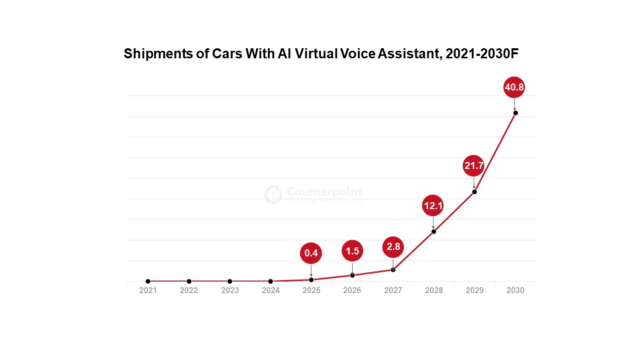
Overall, the potential of natural language voice conversation assistants in cars is vast, and with ongoing research and development, we can expect to see more advanced and sophisticated voice assistants in the future. Developing a successful natural language virtual voice assistant for use in cars is a complex and time-consuming process that requires multiple iterations of training and fine-tuning.
Since the development necessitates a considerable amount of data, computational resources and expertise, only a handful of companies such as Microsoft, Tesla, NVIDIA, Qualcomm, Google and Baidu have the resources to undertake this work. The development of the technology is estimated to take three to four years. There will be an increased demand for vehicles above Level 3.
As highlighted in our report “Should Automotive OEMs Get Into Self-driving Chip Production?”, the automotive industry will confront obstacles related to electrification and intelligent technology, necessitating sustained capital investments and support from semiconductor suppliers. Consequently, only a handful of established car manufacturers with considerable economies of scale will be able to finance these initiatives. The growing popularity of natural voice control in cars will only intensify these challenges.
Related Blogs:
- HERE Maintains Location Platform Leadership; TomTom Surpasses Google to Take Second Position; Mapbox Moves to Fourth
- Mercedes Fends off VW in Europe EV Market
- Qualcomm Gears up to Drive Automotive Industry Transformation
- Qualcomm Bolsters Automotive Presence with One More Deal
- ADAS Penetration Crosses 70% in US in H1 2022, Level 2 Share at 46.5%
- LiDAR Now High on Automotive Industry Radar
Related Reports:
- Should Automotive OEMs Get Into Self-driving Chip Production?
- Global Connected Car Forecast 2019 – 2030F
- Global Automotive NAD Module and Chipset Forecast 2019 – 2030
- Global Automotive ADAS/AD Sensor Forecast by the Level of Autonomy, 2021-2030F
The post AI Voice Assistants to Push Success of Autonomous Driving, Software-defined Vehicle appeared first on Counterpoint.
]]>The post VR Headset See-through Tech to Help in MR Development appeared first on Counterpoint.
]]>
Virtual reality (VR) headsets use real-time six degrees of freedom (DOF) and visual simultaneous localization and mapping (SLAM) to receive real-world information, such as 3D coordinates and object recognition. Initially, the technology was employed for the hand-tracking and Guardian system. Nonetheless, some VR headsets incorporate images from monochrome cameras and, unexpectedly, extend the capabilities of video see-through (VST) to mixed reality (MR). Meta has launched the Quest Pro VR headset, while ByteDance has the PICO4 with full-color cameras to provide MR applications that are more realistic.
The see-through technology used in current VR headsets is called VST, while the see-through technology used in augmented reality (AR) devices is called the optical see-through (OST). The VST technology blends the digitized three-dimensional view of the real world with a computer-generated simulation of reality, which is then shown on the opaque display. By using VST along with the appropriate rendering technique and algorithm, it is possible to enable interaction and occlusion between virtual and actual objects, as well as reconstruct a digital three-dimension model of the physical world.
Unlike VR headsets, which use cameras to obtain the see-through feature, AR devices are manufactured with the see-through capability. The OST function of AR devices allows virtual images to be superimposed directly over real-world vision. The resolution of real-world images in AR devices is significantly higher than in VR headsets. However, current AR devices allow rather limited interaction with the real environment as occlusion cannot be achieved in the absence of depth sensors.
Advantages of VR VST
The VR VST technology allows users to interact with their environment without taking off the VR headset by means of a physical keyboard, mouse, touchpad or controller. It is even capable of creating expensive gadgets in the virtual world, such as multiple displays. Going forward, more experimental AR and MR features will likely be integrated into VR headsets, considerably enriching the ecosystem and usefulness of such devices.
Current challenges faced by VR VST
- Both stereo vision and depth perception are crucial for MR. In the future, VR headsets equipped with a time-of-flight (ToF) sensor will be able to capture more accurate distance information than the camera-equipped ones currently available.
- The VST of a VR headset barely achieves binocular vision. One of the reasons is that there is only one camera for VR VST, which makes it difficult to measure the distance of a close object. Additionally, there will still be warping and distortion of field-of-view objects. Future algorithms must improve this, or designers need to avoid letting users perceive items located closer. Additionally, more color and white balance sensors will be required for making more realistic approximations of the actual color.
- In a novel application of VR, VST technology can be used to bring several displays in the virtual world by creating a few virtual displays. However, the current resolution of virtual displays in VR headsets is less than that in real-world displays. Nevertheless, this issue can be resolved by increasing the resolution of the display on the VR headset, though it would cost more.
- Latency is a crucial characteristic of the VST VR headset because processors must encode the image captured by the camera. Therefore, the speed and bandwidth of processors will affect the performance of VR systems as future mid-range and high-end VR headsets in general will support 4K video streams. Therefore, the VR headset SoC’s requirement should be higher than that of smartphones.
Conclusion
The VST technology in VR headsets can blur the lines between VR and AR, making it possible for VR to provide MR features. MR can be used for numerous purposes apart from just gaming. It can be used in learning platforms, for athletic purposes, webinars and digital twins in the manufacturing industry. Although VR VST still has a few issues that need to be fixed, it can lower the entry barrier for MR applications. Increasing adoption by users and developers can help in the improvement of the VR headset VST technology, which will lead to the creation of more MR apps. In turn, these MR apps will drive the development of AR hardware and ecosystems. After all, AR devices have certain advantages that cannot be replicated by VR devices.
Related Posts
- AjnaLens: India-based XR Startup Upskilling Workforce Training with VR & Metaverse
- Global XR (AR & VR Headsets) Shipments Market Share: By Quarter
- Meta’s New Quest Pro: More Attractive to Enterprises Than Gamers
- Podcast: XR – Where are We in Reality?
- Snapdragon Summit 2022 Day 1: Qualcomm Snapdragon 8 Gen 2 mobile platform with new AI experiences, real-time ray tracing, Wi-Fi 7 announced
- XR (VR/AR) Headset Shipments to Grow 10 Times to Cross 100 Million Units by 2025
The post VR Headset See-through Tech to Help in MR Development appeared first on Counterpoint.
]]>The post A Promising Yet Challenging Market for Self-driving SoCs appeared first on Counterpoint.
]]>Semiconductors are becoming more important for automobiles as electrification and intelligence continue to advance. Among these, the level of intelligence has emerged as an essential factor that customers consider when buying a vehicle. The accuracy and efficiency of autonomous driving are determined by the computational capabilities and manufacturing process of the chip. Therefore, the increase in demand for autonomous driving is pushing the demand for advanced processes and will significantly increase the market size of advanced driver assistance systems (ADAS)/Autonomous driving (AD) chips. The computational capability of ADAS/AD processors must meet the requirements of the corresponding autonomous driving level. The Society of Automotive Engineers (SAE) defines the various levels of autonomous driving as follows:
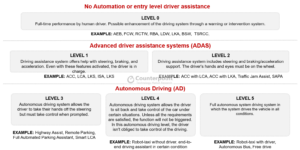
The TOPS (trillion operations per second) of Level 2 ADAS/AD chips is typically between 10 and 100, but the TOPS of Level 3 is between 150 and 200 and the TOPS of Level 4/Level 5 is more than 400 and will reach 1000+. Each level is divided further based on functionality. Basic Level 2 features include only adaptive cruise control (ACC) and lane-keeping system (LKS), and can be achieved by an SoC with only 10 TOPS. However, advanced Level 2 may require up to 75 TOPS to achieve advanced ACC, which can maintain the lane center and pre-control the speed at upcoming curves.
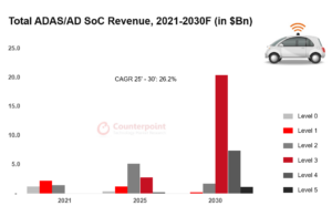
The global ADAS/AD SoC market is expected to reach $30 billion by 2030 with a CAGR of 26.3% between 2022 and 2027. SoCs in the Level 2 category will have a revenue market share of 44.4% in 2022, which will reach a record high of 60% in 2024 due to an increase in safety requirements and a decrease in component prices. Level 3 AD systems will take a few years to gain the public’s trust, but by 2027, they will replace Level 2 as the standard. Compared to Level 3 SoCs, Level 4 SoCs have greater computational capability and bandwidth to process more high-resolution images and make a quick response. As a result, the entry barrier and cost of Level 4 SoCs are much higher than those of Level 3 SoCs, hence they will mostly be utilized in luxury vehicles and robotaxis.
The entry barrier to Level 1 and Level 2 ADAS SoC is low. Therefore, ADAS penetration can increase significantly when the cost of ADAS sensors, such as cameras and radars, continues to decline. Counterpoint expects that the global penetration of ADAS in car shipments will reach 78.7% by 2024. At the same time, multiple new players will enter the ADAS chip market. These startups are capable of AI chip design and mass production, and their solutions can swiftly fulfill localized requirements, such as local language and localization algorithms, at competitive prices. Therefore, emerging car OEMs will favor these new solutions. However, traditional automotive chips, such as Renesas and NXP, are also providing solutions. Level 3 employs more sensors and more efficient computing units than Level 2. The most significant difference between Level 3 and Level 4 is the improvement in artificial intelligence, as Level 4 autonomous vehicles must be able to take rapid decisions.
On the other hand, the development of autonomous driving (AD) chips is primarily driven by established consumer electronics giants such as NVIDIA and Intel (Mobileye). The R&D expenditures and entry barriers for AD chips are significantly greater than those for ADAS. In addition to the core AI chip, AD solutions should also incorporate connectivity, sensing systems, image training models, ADAS map development, route planning, vehicle control, driver monitoring systems (DMS), natural language processing (NLP) and intelligent cockpit solutions. Moreover, the AD chip must be able to deliver tailored and region-specific algorithms. This must be accomplished through the collaboration of automotive OEMs and AD chip companies. All of these factors make it challenging to create a good AD chip and the payback time is also lengthy.
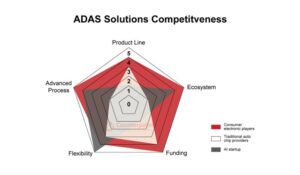
Advantages, Disadvantages Faced by 3 Primary ADAS/AD Chip Vendors
In the past, there used to be a distinct division of labor between car OEMs, Tier 1 suppliers and chip vendors (Tier 2). The chip vendors might be either fabless firms or IDMs, and both would place orders to the foundry. Since the demand for semiconductors in the automotive industry was modest and all semiconductors used in automobiles were manufactured with mature processes, the foundry was less important. However, the performance and features in future automotive processors will play a crucial role in migrating to autonomous driving and electrification. Consequently, the ecosystem of collaboration between OEMs, Tier 1 suppliers and chip manufacturers is beginning to shift. Chip providers which were once Tier 2 are beginning to collaborate directly with OEMs. In addition, these three types of companies may engage directly with foundries to secure chip sources.
Competitor landscape
Mobileye is the leading Level 1 and 2 supplier due to its early entry. However, because of a lack of flexibility and superior alternatives, Chinese automakers want to replace Mobileye with NVIDIA or Horizon robots. Additionally, its solution has less computational power than those of its competitors. To keep up with other companies, Mobileye also introduced at CES 2022 its EyeQUltra, EyeQ6 Light and EyeQ6 High SoCs for L4, L2 and L1/L autonomous driving, respectively.
NVIDIA has aggressively entered the automobile autonomous driving market with its expertise in GPUs for the AI business. The benefits of NVIDIA’s AD processors include high computational power, extensive software tools and a complete environment allowing clients to create their own algorithms. In terms of clientele, NVIDIA works with the majority of automakers and Tier 1 suppliers worldwide. Atlan, the most recent AD chip from NVIDIA, has been released in 2022 with 1000 TOPS of computational capacity and is expected to enter mass production by 2025, aiming at L4/L5 autonomous driving solutions.
Qualcomm is a pioneer in smart cockpits but a follower in autonomous driving technology. Qualcomm’s Snapdragon Ride, a high-performance, low-power autonomous driving solution that supports L1-L5 degrees of autonomy, is aimed at the mid-to-high-end autonomous driving market.
Horizon Robotics, one of the few autonomous driving chip solution vendors in China, will likely supply to Chinese automakers in the coming years. Horizon has positioned itself as a competitor to Mobileye and NVIDIA. A new participant in the industry, it has introduced many products that correspond to Mobileye’s solution. In contrast to NVIDIA’s general-purpose processors, Horizon’s AD SoCs are ASICs, which consume less power and are more efficient than general-purpose CPUs. However, they are less flexible and may experience the same difficulty when moving to Level 3 and beyond.
Related Posts and Reports
- Global Automotive Semiconductor Forecast by the Level of Autonomy, 2021-2030F
- Global Autonomous Passenger Vehicle Market 2019-2030
- Automotive LiDAR Market Trend and Implications 2022
- Qualcomm in Driver’s Seat To Shape The Future of Mobility
- Connected Vehicle 2022 Summit: From ADAS to Autonomous Mobility, Here are Some Key Takeaways
- One in Two Cars Sold Will Have Electric Powertrain by 2030
- HERE Maintains the Location Platform Leadership, Ahead of Google, and TomTom in 2021
The post A Promising Yet Challenging Market for Self-driving SoCs appeared first on Counterpoint.
]]>The post Ukraine Crisis Brings Fresh Wave of Uncertainty to Semiconductor Industry appeared first on Counterpoint.
]]>The market is apprehensive the Ukraine crisis will result in shortages of key raw materials, eventually affecting the semiconductor supply chain. Besides, financial sanctions have blocked Russia‘s foreign trade and major semiconductor foundries have stopped shipping to Russian customers. All this has created new uncertainties for the hard-won recovery of semiconductor trade. The result and the extent of this non-economic event are unpredictable. But it has already started affecting the supply chain. In the following lines, we will provide a quick analysis of potential supply disruptions in the semiconductor industry based on the current status.
Some raw materials exported from Russia and Ukraine, such as rare gas neon, chemical C4F6 and metals palladium, nickel, platinum, rhodium and titanium, are critical for semiconductor manufacturing.
A neon gas mixture is commonly utilized as a light source in the ArF and KrF excimer lasers for lithography. The chemical C4F6 is used in the etching stage. Since the semiconductor process for 3D structures needs a significant number of etching steps, the shortage of C4F6 will have a bigger impact on 3D NAND production than on foundry logic fab.
However, we should note that neon prices soared by more than 10x during the 2014 Crimean crisis in Ukraine even as the semiconductor industry cut the total usage of the gas by 20%-40% after adjusting software logic and optimizing the purging process of the gas filling procedure. Therefore, the supply chain will be impacted if the gas manufacturing facilities are destroyed during the current war. If not, we may still see rising prices, though the impact on production will remain manageable.
However, the gas and chemical produced in Russia and Ukraine are not exclusive to the region. The manufacturing sites are limited because the production involves high energy consumption and environmental pollution. But if prices rise rapidly and demand remains strong, there will undoubtedly be more players entering the market in other parts of the globe.
Palladium is used in component production, like for the substrate in PCB. However, precious metals such as palladium, platinum and rhodium are mainly used in the catalytic converters for vehicles. Titanium nitride (TiN) is a widely used material for semiconductor manufacturing as a diffusion barrier. The world’s second-largest exporter of titanium is Russia (the US is No.1). The production of lithium batteries may also face some turbulence because nickel, of which Russia is a major producer, is an important metal for these batteries
Implications:
- The short-term risk of supply shortage comes not only from wars and bans but also from trading. Trading with other nations has become extremely difficult for Russia due to its exclusion from SWIFT and worsening inflation.
- In the medium term, the lack of the aforementioned raw materials will have little influence on semiconductor producers. The situation will be managed through existing inventory and other suppliers. However, it is inevitable that prices will rise significantly.
- Larger enterprises have more purchasing power. Small and medium chipmakers and allied businesses may face increased supply pressure owing to exhausted inventories and the difficulty in connecting with new sources if the conflict continues.
- In the long run, small and medium chip producers may place multiple orders to offset this risk, resulting in the raw material supply to deteriorate.
- Rapidly rising metal (nickel and palladium) prices will represent a new impediment to the revival of the automotive market if the conflict continues.
- With geopolitical tensions now extending from Asia to Europe and from semiconductor manufacturing to raw material supply, capacity expansion and investment decisions will have to be reevaluated.
- The upstream supply chain, as well as semiconductor manufacturers, will be encouraged to go local, which implies higher costs.
- If the conflict persists, supply chain uncertainty will keep raw material inventories at higher levels for a longer length of time. Supply chain management will become more complicated as well.
Related Posts
The post Ukraine Crisis Brings Fresh Wave of Uncertainty to Semiconductor Industry appeared first on Counterpoint.
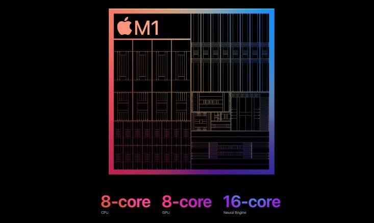
]]>The post M1 Pro, M1 Max Give Definitive Push to Apple’s M1 Journey appeared first on Counterpoint.
]]>Following up on our May coverage of Apple’s M1 SoC introduction, we look at the benefits and downsides of the new M1 Pro and M1 Max SoCs, released on October 18 along with the updated MacBook Pros carrying these SoCs. These launches come around one year after the introduction of the M1 Mac.
Apple has mastered both its software (OS and APP) and hardware system architectures, thanks to its years of experience in designing RISC SoCs for its smartphones and tablets. The success of the M1, Apple’s first high-performance SoC for entry-level Macs, prompted the company to accelerate the development of more advanced SoCs.
Unlike Intel’s general-purpose processors, which can be used in different notebook models and brands, Apple’s M1 series SoCs are an ASIC (application-specific integrated circuit) that can be only used in Apple-designed PCs. The M1 Pro and M1 Max SoCs have more high-performance cores. However, the number of high-efficiency cores is reduced to two from the M1’s four. Both are made by TSMC’s 5nm technology.
Comparing M1 Pro, M1 Max, M1 and A15
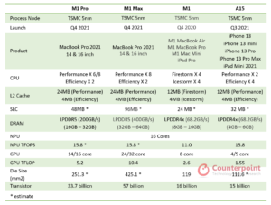
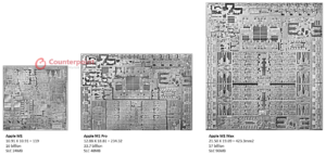
Apple did not share any information about the new CPU core or frequency. According to information presented by TSMC at the 26th Technology Symposium, the N5P is 5% faster and 10% more energy efficient than the N5, although the transistor density has not improved as a result. The M1 Pro and M1 Max, according to Apple, have a transistor of 33.7 billion and 57 billion, respectively. As a result, the die size of the M1 Pro and M1 Max will be close to 251.3 mm2 and 425.1mm2, respectively. Both have broken die size and transistor count records for Apple’s products.
Source: Apple
This evolution of the M series chips is in line with Apple’s processor development strategy. Working closely with TSMC, Apple will see significant chip improvements every two years. In addition to the Ax chips for smartphones, Apple also created M series chips for PCs in 2020, with the goal of replacing all Intel CPUs with Apple Silicon within two years. The SoC architectures in iPhones, and iPads and Macs are similar but the Mx for PC has more cores and larger cache memory. In other words, Apple’s latest and most advanced processor will be the Mx for PCs instead of the Ax for smartphones. Ax will inherit the features and innovations of the Mx and become its customized version.
SLC (system-level cache)
From the die shots of both the M1 Pro and M1 Max from Apple, the SLC is estimated to reach 48MB and 96MB, much larger than the 32MB of the A15 Bionic and the 24MB of the M1. Apple has boosted the cache capacity to improve system performance while lowering power consumption at the cost of die size. To enhance system efficiency, this SLC can be shared among multiple SoC subsystems (like CPU and GPU cores). Further, the bigger cache can reduce the frequency with which the SoC accesses DRAM, lowering system power consumption, requirement for DRAM and, in turn, the BOM.
Apple has been expanding its APIs for new applications including gaming, ray tracing and augmented reality/virtual reality. All these applications necessitate SoCs with several cores that communicate and collaborate with one another, as well as huge system caches to improve responsiveness.
Powerful GPU
GPU is the key to demonstrating the capacity of new chips. The M1 Pro and M1 Max have 16 and 32 GPU cores, respectively. GPUs, unlike CPUs, are made up of a large number of tiny cores. Initially, GPUs were designed to speed up specific 3D graphics operations but they are now capable of rendering increasingly realistic 3D visual effects, such as light tracing. Since the introduction of 3D graphics, light tracing has been one of the most significant advancements in the field of graphics technology. It is also a crucial technique for designing AR/VR/XR scenes. Light tracing, which may be utilized in embedded segments such as mobiles, wearables, gaming and automotive, is now critical to the realism of any 3D environment.
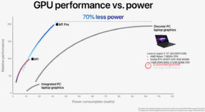
The GPU of the M1 Pro has 16 cores and only 5.2 TFLOP. However, Apple claims that the M1 Pro’s GPU delivers comparable performance within certain power consumption to the discrete GeForce RTX 3050 Ti 4GB while using 70% less power. Counterpoint believes this is due to the SoC’s huge quantity of shared cache in both Level 2 cache and SLC. Furthermore, the GPU can make use of the shared 32GB of LPDDR5, which is significantly more than the RTX 3050’s 4GB of GDDR6.
Ray tracing is a technique that was heavily emphasized at the Apple Worldwide Developers Conference (WWDC) in 2020 and 2021. At the 2021 WWDC, the training related to its inclusion in gaming accounted for 32.4% of all technological training sessions, making it the top training topic. To fully realize the capabilities of ray tracing, these APIs require GPU support.
The GPU may also be utilized as a more flexible parallel processor, supporting a wide range of AI applications. At the 2017 WWDC, Apple announced Core ML, which allows developers to create tethered applications for Apple devices. GPU support is required for Core ML. Specific applications such as AR, gaming and imaging are among the applications that Apple will emphasize currently and in the near future.
Source: Apple
Memory architecture
LPDDR5 is used in both the M1 Pro and M1 Max, with bandwidths of 200 GB/s and 400 GB/s, respectively, which are significantly faster than the M1’s 68.2 GB/s. Apple Silicon’s memory architecture is undoubtedly one of its greatest strengths. The M1 Pro and M1 Max share the same UMA to embed high-bandwidth and low-latency DRAM into a single pool within a custom package. Therefore, all cores can retrieve data in the memory simultaneously, and the system can dynamically arrange the precious memory resource. This dramatically improves system performance and reduces the usage of power-hungry DRAM, consequently extending the battery life.
Use cases for M1 Pro and M1 Max
- Content creators are undoubtedly the largest target group for the M1 Pro and M1 Max. The M1 series Mac can be supported natively by most video/photo-editing software for Mac. Most third-party software, such as Adobe Photoshop and Lightroom, performs faster with the Rosetta2 compatibility while consuming less power on the M1 Pro and M1 Max.
- Game developers are among the M1 Pro and M1 Max’s potential customers. As previously stated, one of the primary sources of revenue for Apple’s store service is games. However, Intel-based Macs were previously seen as unsuitable for playing high-quality games due to their hardware’s inability to meet the demands of gaming, let alone AR/VR/XR games. Classic games will be ported to native ARM architecture thanks to the M1 Pro and M1 Max’s much improved GPU, and it will encourage more developers to do the same. Apple has also provided APIs and training for 3D situations such as light tracing at recent WWDCs. These are essential technologies for game production as well as the construction of AR/VR/XR scenarios.
Conclusion
- Apple’s M1 Pro and M1 Max meet the company’s requirements for a multitasking, high-performance and power-efficient mid-to-high range laptop. According to Counterpoint estimates, Apple Silicon is currently powering 93% of Macs. As new chips are launched, this proportion will continue to grow.
- Apple’s new Macs are intended to appeal to a wide range of customers, including content creators, game designers, gamers and early adopters. Apple’s next silicon upgrade is likely to include additional high-performance CPU cores to improve multitasking, more GPU cores to improve the performance of video editing and gaming, and AI training capability.
A detailed report, ‘Apple M1 Pro and M1 Max Macs Review’, will be available by the end of October on our website for paying subscribers.
Related Reports
- Apple Unleashes MacBook Pros with New M1 Pro, M1 Max SoCs, Promises a Notch Higher Performance
- Apple M1 Macs Review
- Smartphones Memory Historical data and Forecast, Worldwide Demand, 2018-2024
- How 5G, AI and IoT are Shaping Future of Storage
- Storage Capacity Requirement for Autonomous Vehicles in the Next Decade
Related Posts
- No Stopping This Apple Cart: New Macs to Extend Chip Dominance
- One in Five iPads Sold in 2022 to Have Apple’s M-series SoC
- Average Smartphone NAND Flash Capacity Crossed 100GB in 2020
- Smartphone Storage Capacity Zooms on Increased Demand
- Three Improvements Apple Made for Cameras of its iPhone 12 Pros
- Apple Silicon Set to Energize PC Market as Possibilities Beckon
- Apple ‘Arms’ Macs with Apple Silicon
The post M1 Pro, M1 Max Give Definitive Push to Apple’s M1 Journey appeared first on Counterpoint.
]]>The post Mobile Demand Raises DRAM Revenue by 30% YoY to $19 bn in Q1 2021 appeared first on Counterpoint.
]]>Global DRAM revenues rose to $19 billion in Q1 2021, increasing by a solid 30% YoY and 9% QoQ. Distance education and work from home (WFH) continued propelling a substantial demand for smartphone and laptop DRAM, resulting in a 6% growth in bit shipment and a 3% rise in ASP over the previous quarter.
Associate Director Brady Wang said the Chinese handset makers stepped up their smartphone shipments in the first quarter, intending to gain shares from the beleaguered Huawei. In addition, the high-density LPDDR4x memory prices softened in H2 2020, increasing smartphone DRAM content and making 6GB the minimum standard for mid- to high-end smartphones since 2021. As a result, the average DRAM capacity in smartphones clocked at 5.3GB in Q1 2021, rising impressively by around 21% YoY and 7% QoQ. Similarly, servers experienced recovery in demand, and the adoption of a new data-center CPU bumped up server content per box. Therefore, the server segment’s DRAM demand rose as well.
According to Wang, DRAM is already an oligopolistic market with an Herfindahl-Hirschman Index (HHI) of 3,138. A significant capacity expansion by any player will soon turn around market status and reduce the overall profitability. Therefore, this year, all three major players will spend most of their resources in migrating to advanced nodes, a process that is bound to reduce production capacity. In addition, transportation and component shortage concerns will force device vendors to place orders earlier than usual. When coupled with the growing demand for personal computers, games and servers, these factors signal the possibility of the DRAM market turning to a shortage this year. The smartphone market is recovering at present, but its cost sensitivity means that a DRAM price spike may put the brakes on smartphone DRAM content growth.
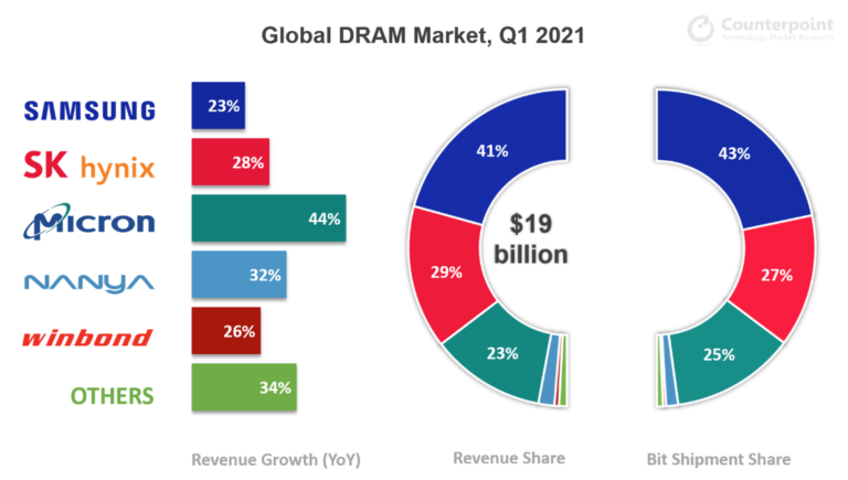 Competitive Landscape
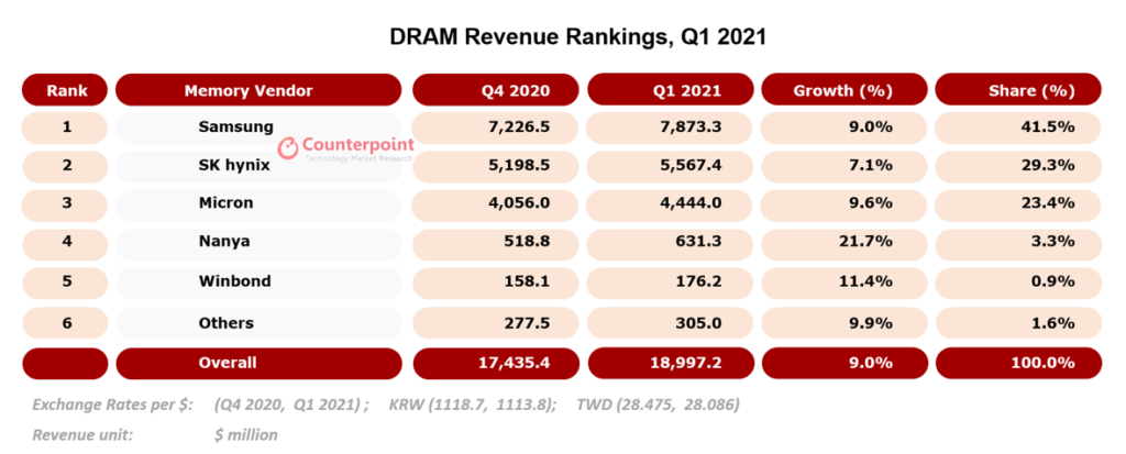
The DRAM industry is dominated by three major players that collectively account for about 95% of the market’s bit shipments and revenue.
Samsung Electronics
With $7.9 billion in revenue, Samsung led the DRAM market in Q1 2021. The South Korean semiconductor giant continued commanding over two-fifths of the DRAM market revenue, overshadowing its nearest competitor by over 41%. Samsung’s DRAM bit shipment growth came from actively responding to the (i) 5G-related surge in smartphone demand, (ii) rising server demands for data centers and (iii) rise of home entertainment culture that increased memory content in TVs and STBs to support 4K UHD content and streaming.
Research Associate Siddharth Bhatla sees 1Z nm or 15 nm as Samsung’s most advanced mass-produced DRAM node from the technology perspective. The company’s plans include beginning mass production of 14 nm node in H2 2021. Samsung aims to differentiate its DRAM offerings using multi-layer EUV on its 14 nm node, building upon the single-layer EUV in its current 15 nm node.
SK hynix
Ranking second, SK hynix accounted for over 29% of the DRAM industry’s Q1 2021 revenues. Surpassing Micron by over 25%, its revenues rose by over 28% YoY in that period, in line with the industry’s overall growth. In addition, the company’s bit shipments rose 4% QoQ, thanks to its ability to actively cater to the surging demand for mobile and PC memory. By the year-end, SK hynix aims to (i) ramp up the production of its 1Z nm DRAM and (ii) complete development and begin mass production of its 1α-EUV node.
Micron Technology
Micron achieved a 44% YoY jump in its DRAM revenue in Q1 2021, continuing to grow fastest among the big three since the preceding two quarters. Micron was the first among the big three to begin mass production of 1α DRAM, accounting for one-fourth of the industry’s DRAM revenue. However, Micron’s 1α node is based on DUV, an older technology that may face severe cost competition once the EUV-based 1α DRAMs reach the mass market.
Feel free to contact us at press(at)counterpointresearch.com for questions regarding our in-depth research and insights, or for press enquiries.
Background:
Counterpoint Technology Market Research is a global research firm specializing in products in the TMT (technology, media and telecom) industry. It services major technology and financial firms with a mix of monthly reports, customized projects and detailed analyses of the mobile and technology markets. Its key analysts are seasoned experts in the high-tech industry.
Brady Wang
![]()
Siddharth Bhatla
![]()
Counterpoint Research
press(at)counterpointresearch.com
![]()
Related Reports
- Apple M1 Macs Review
- How 5G, AI and IoT are Shaping Future of Storage
- Smartphone NAND Flash Status Update, Q4 2020
- Smartphone DRAM Status Update, 2020 Q4
- Smartphones Memory Historical data and Forecast, Worldwide Demand, 2018-2024
- Storage Capacity Requirement for Autonomous Vehicles in the Next Decade
- Global Smartphones NAND Memory Tracker and Forecast by Brand, Capacity & Interface: Q1 2019
The post Mobile Demand Raises DRAM Revenue by 30% YoY to $19 bn in Q1 2021 appeared first on Counterpoint.
]]>The post NAND Flash Recovery Begins on Rising Demand and Supply appeared first on Counterpoint.
]]>- In the first quarter of 2021, the NAND flash memory market rebounded by 4.6% QoQ to $15.3 billion, while bit shipment increased by 12%.
- Leading manufacturers are developing new NAND flash with additional layers to lower bit density and increase manufacturing efficiency. In the first quarter of 2021, the bit shipment growth for the layers 64 to 130 climbed by over 20%.
- Samsung dominated the NAND market revenue share, SK hynix achieved the highest QoQ growth in revenues, and Micron led the industry in the volume production of 176-layer NAND flash.
Global NAND flash revenues increased 4.6% in Q1 2021 to $15.3 billion over the previous quarter. Distance education and remote working propelled the demand for notebook SSDs, which helped the big players in offsetting the reduced NAND flash demand from the server and data center market.

Associate Director Brady Wang said the continued expansion of smartphone storage capacities, particularly by the Chinese OEMs, created an unusual scenario for NAND flash usage. The average capacity of smartphones climbed 6% in Q1 2020, according to Counterpoint data. As a result, contract prices for NAND flash fell by 4-7% in Q1 2021, which is much lower than the 7-11% drop in Q4 2020. The decrease eased in late Q1 2021. In the same period, NAND flash spot prices fell 1-3% but started increasing by that quarter’s end.
Wang added that in Q1 2021, memory vendors were in full force migrating to more layers. Bit shipment increased 12% QoQ, while overall ASP decreased 6% in the same period. In terms of layers, the ratio of bit shipment for the layers 64 to 130 increased from 52% in Q1 2020 to 81% in Q1 2021. This increase in layer count allowed an annual reduction in NAND costs by an average of 20%, which however is less than the historical 30%. Ideally, NAND flash can reach more than 500 layers. However, in reality, the NAND flash production starts encountering several challenges after 100 layers, like a high aspect ratio and long manufacturing time. As a result, vendors adopt Core Over Periphery (COP)/Circuit Under Array (CUA) to reposition the logic circuit to below the memory cell. Doing so allows them to increase the number of net per wafer. Also, double stacking can help increase the number of layers quickly but may result in higher costs due to lower yields.
On the handset side, key NAND flash players are proactively marketing the high-density uMCPs at advantageous costs. Chinese smartphone MCP densities rose from 8GB/128GB to 12GB/256GB over the previous quarter.

Competitive Landscape
Currently, the NAND flash industry is dominated by six major players. This landscape is likely to undergo a major rejig in the near term, given the ongoing acquisition of Intel’s non-volatile memory solution unit by SK hynix.

Samsung
Samsung led the NAND market in Q1 2021 with $5.1 billion in revenues, overshadowing its nearest competitor by over 80%. The South Korean electronics giant continued accounting for over one-third of the NAND market revenue for the fifth consecutive quarter. The weakness in US dollar against the Korean Won worked out negatively for the company’s component business, but it was fully compensated by its end-user product business.
Samsung is migrating to the 128-layer 6th generation V-NAND, aiming to use this technology in the near term for driving its bit growth and cost competitiveness. Samsung’s single-stack process in the 128-layer 6th generation V-NAND allows it to have lower costs than competitors which use a double stack. However, the company will adopt its 7th generation V-NAND, a double stack-based 176-layer memory, later this year to reinforce its technological competitiveness at the cost of decreasing profit margin.
SK hynix
SK hynix’s revenues from NAND achieved a good 12% QoQ growth in Q1 2021 despite enduring a 7% drop in its ASP. This stellar performance stems from (i) the sales growth of its high-density smartphone memory products, and (ii) enhanced cost competitiveness of the company’s major products powered by yield improvements.
Research Associate Siddharth Bhatla said SK hynix achieved a bit shipment growth of a whopping 21% in Q1 2021, which was over double of the same for WDC and Samsung. The company expects the NAND market’s bit demand growth to be in mid-30% over 2021, which it plans to cater proactively in this year’s second half. By this year-end, the company plans to raise its NAND product mix of 128-layer to 80% and begin the mass production of 176-layer node.
WDC
Ranking third in revenue, WDC is the only NAND flash manufacturer that also makes HDDs. The company’s portfolio in laptop SSDs helped it benefit from the surge in PC demand, resulting in an 8% increase in its QoQ bit shipments in this quarter. The company’s diversified end-market portfolio in client devices and solution experienced a revenue growth of 10% and 8% respectively, balancing its 20% revenue decline in the data center market.
Micron
Micron is leading the NAND industry’s 176-layer node, having begun its volume production during the past quarter, which is ramping up considerably over time. Micron plans to make this node the company’s workhorse for 2022, augmenting the company’s bit growth and long-term cost reduction strategy. The company is focusing on increasing the mix of QLC NAND in its product portfolio. This technology’s cost-effectiveness is driving the transition of the compute memory industry from HDDs to SSDs.
Micron has positioned itself to capitalize on the booming demand for non-volatile memory products, which is created by the increased adoption of AI and 5G around the world’s data centers, intelligent edge and user devices.
Feel free to contact us at press(at)counterpointresearch.com for questions regarding our in-depth research and insights, or for press enquiries.
Background:
Counterpoint Technology Market Research is a global research firm specializing in products in the TMT (technology, media and telecom) industry. It services major technology and financial firms with a mix of monthly reports, customized projects and detailed analyses of the mobile and technology markets. Its key analysts are seasoned experts in the high-tech industry.
Analyst Contacts
Brady Wang
![]()
Siddharth Bhatla
![]()
Counterpoint Research
press(at)counterpointresearch.com
![]()
Related Reports
- How 5G, AI and IoT are Shaping Future of Storage
- Smartphone NAND Flash Status Update, Q4 2020
- Smartphone DRAM Status Update, 2020 Q4
- Smartphones Memory Historical data and Forecast, Worldwide Demand, 2018-2024
- Storage Capacity Requirement for Autonomous Vehicles in the Next Decade
- Global Smartphones NAND Memory Tracker and Forecast by Brand, Capacity & Interface: Q1 2019
Related Posts
- Smartphone Storage Capacity Zooms on Increased Demand
- Average Smartphone NAND Flash Capacity Crossed 100GB in 2020
- Expected Memory Market Rebound in 2020 and Continuous Investment Can Strengthen Samsung’s Leading Position in Memory
- SK Hynix to Cut DRAM Production and Reduce Wafer Start of NAND Flash
The post NAND Flash Recovery Begins on Rising Demand and Supply appeared first on Counterpoint.
]]>The post No Stopping This Apple Cart: New Macs to Extend Chip Dominance appeared first on Counterpoint.
]]>On November 10, 2020, Apple introduced three new Mac devices — MacBook Air, MacBook Pro and Mac Mini. On April 20, 2021, Apple debuted the new iMac. All these are powered by the Apple M1 SoC. Apple has mastered both its software (OS and APP) and hardware system architectures, thanks to its years of experience designing customized RISC SoCs for its smartphones and tablets. Apple would like to extend this advantage to its future PC chips. As a result, Apple’s first high-performance SoC and architecture for the entry-level Mac has demonstrated its dominance over rival devices in its class.
Unlike Intel’s general-purpose processors which can be used in different models/brands of notebooks, Apple’s first SoC for Macs, the M1, is an ASIC (application-specific integrated circuit) to be only used in Apple-designed PCs. However, it can satisfy more than 80% of the requirement for entry-level PCs. In addition, Apple’s customized high-performance core (Firestorm) has many advantages over other ARM SoCs and x86 CPUs, such as high-density L1-L3 cache, eight-bit decoder, eight transmit (Dispatch) and 630 ROB.
Apple has added many dedicated cores which have better computing performance and less power consumption. Developers can enjoy both the benefits as long as they design their apps based on the APIs provided by Apple. The integration of these cores in a single SoC results in significant cost savings and provides additional features. These investments are expensive but provide solid and differentiated functionalities that are difficult for competitors to deal with.
Apple’s motivation for releasing new Macs
Apple intends to build an updated PC ecosystem based on the popularity of Apple chips in the iPhone and iPad. Furthermore, the new chips have the potential to unify the architecture of the iPhone and Mac, resulting in a unified ecosystem that Apple can completely control. M1 Macs will run iOS (iPhone and iPad) apps, with Apple’s Catalyst project enabling iOS and macOS developers to share code. Some apps are likely to be incompatible with the new framework due to the switch from Intel processors to Apple Silicon. More native iOS apps are expected to move to the macOS over time.

Advantage of new Macs over Intel CPU-based counterparts
- Power saving/always on/fast booting speed: The latest M1 Macs’ architecture is similar to the iPhones’. In the MacBook Air, Apple has replaced the fan with a passive cooler. Active cooling (fan) is present in the MacBook Pro and iMac, but it is seldom used, minimizing the amount of energy lost. ‘Always on’ devices will go from standby to active mode in a matter of seconds.
- Running iOS apps on macOS: Developers can easily port apps from the iOS platform to the Mac using Mac Catalyst. ‘Continuity’ allows iOS and macOS devices to communicate easily and seamlessly for a better user experience.
- Enhanced AI capability: The iOS 11, launched in 2017, included machine-learning APIs and Core ML. Core ML turns existing server-trained models into Core ML models. A Core ML model that has been optimized will run many times faster.
- Faster data access speeds in storage: The storage design of the M1 Mac is identical to that of the iPhone. Apple has used the Non-Volatile Memory express (NVMe) communications protocol since the iPhone 6s, which provides considerably faster storage than its rivals. OSX (iOS, macOS) can also aid in data fragmentation reduction and access speed improvements.

Suitable use cases for M1 Macs
- Basic usage and office applications: Outlook, Word, Excel, PowerPoint and OneNote now can all run natively on the M1 Mac to take advantage of performance improvements. M1-based Excel VBA runs three to four times faster than on x86 CPUs, making it faster than on Intel processor-based Macs, according to our measurements.
- Content creators: Most video/photo editing applications for Mac can support M1 Mac natively, or at the very least via Rosetta2. Adobe Photoshop and Lightroom have seen significant efficiency, power, and memory consumption improvements.
- Programmers: The M1 is designed to work with Xcode to create macOS or iOS apps. For this reason, many third-party libraries must be recompiled. The M1 is the new currency.
Benefits of new Macs
Apple moved to new Mx SoCs for a variety of reasons. Cost was one of them but not the most significant. Moving to a system architecture takes time, but there are several benefits in terms of hidden costs:
- Increase in the quantity and consistency of Mac Apps: Apple would make it possible for iOS and macOS to share tools and architecture, allowing iOS developers to work on macOS as well. The aim is to make applications run smoothly on both platforms. The new framework will also pass the iPhone and iPad user experience.
- Reduction in the number of chips outsourced: Apple’s use of in-house SoCs has allowed the company to build an ecosystem that is not dependent on chip partners such as Intel and AMD. It also means Apple will be able to better handle software-hardware vulnerabilities.
- Increase in service revenue: Apple’s service revenue has grown rapidly over the past five years, with a five-year CAGR of 21.8%. Apple’s continuous introduction of new hardware helps increase the stickiness of its products, which in turn raises service revenue. Apple’s censorship also helps maintain the platform’s security, and will encourage more developers to sell their apps in Apple’s marketplace.
Future Apple Silicon and Macs
We believe the M1 is seen by Apple as the Apple Silicon for entry-level Macs. We expect Apple to launch an Apple Silicon upgrade for the MacBook Pro in Q4 2021 to differentiate it from the MacBook Air and the next Apple Silicon in 2021 for the iMac Pro. The new Apple Silicon is likely to use TSMC’s 4nm process for cost reduction and efficiency improvement. The primary goal of the Apple Silicon for MacBook Air and MacBook Pro would be to have a balance between performance and power consumption. The highly integrated PCB and the laptop-grade SoC, which is smaller than Intel’s CPU, can reserve more space for battery packs. However, Apple Silicon for desktop would need high-performance CPU cores, plus the improved NPUs and GPUs. Conversely, in situations where battery life and chip size are not major concerns (like in a desktop Mac), the chip’s performance can be maximized.
A detailed report, ‘Apple M1 Macs Review’, is available on our website for paying subscribers.
Related Reports
- Apple M1 Macs Review
- Smartphones Memory Historical data and Forecast, Worldwide Demand, 2018-2024
- How 5G, AI and IoT are Shaping Future of Storage
- Storage Capacity Requirement for Autonomous Vehicles in the Next Decade
Related Posts
- One in Five iPads Sold in 2022 to Have Apple’s M-series SoC
- Average Smartphone NAND Flash Capacity Crossed 100GB in 2020
- Smartphone Storage Capacity Zooms on Increased Demand
- Three Improvements Apple Made for Cameras of its iPhone 12 Pros
- Apple Silicon Set to Energize PC Market as Possibilities Beckon
- Apple ‘Arms’ Macs with Apple Silicon
The post No Stopping This Apple Cart: New Macs to Extend Chip Dominance appeared first on Counterpoint.
]]>The post Taiwan Drought May Worsen Global Component Shortage appeared first on Counterpoint.
]]>Taiwan dominates semiconductor production globally due to its unique position in the foundry and outsourced assembly and testing (OSAT) industry. Semiconductor mass production also uses some of the most advanced technologies which make setting up a production unit a high-investment and time-consuming affair. This is why the current drought in Taiwan has set alarm bells ringing the world ever.
According to Counterpoint’s Foundry Service, TSMC’s foundry market share reached 58.6% in 2020, equivalent to an HHI of 3,798. By production region, Taiwan’s foundry market share, including TSMC, UMC, VIS and PSMC, reached 68.9% in 2020, with an HHI of 5,098. In addition, there are memory fabs including Micron Technology, Nanya Technology, Macronix and Winbond. These semiconductor fabs are located in three major technology parks in the country (see Exhibit 1).
Exhibit 1: Reservoir Capacity of Taiwan’s Major Science Park Sites
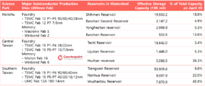
Data source: Counterpoint semiconductor factory database
Reservoir data source: https://water.taiwanstat.com
A stable and quality source of water is essential for semiconductor production. However, Taiwan is currently suffering from its worst drought in 56 years due to less than usual rainfall during the past year. The main sources of water in Taiwan are (1) the plum rains that occur in spring and summer when hot and cold air meet, (2) the heavy rainfall from typhoons in summer, and (3) the light rainfall in the mountains from the northeast monsoon in fall and winter. The proportions here are about 12%, 39% and 6% respectively.
Taiwan usually receives 7-9 typhoons every year. However, only one typhoon landed in Taiwan in 2020. To make matters worse, last winter and spring’s rainfall was heavily deficient, causing a shortage of water in Taiwan. The country is topographically divided by the 3,000-metre-high Central Mountain Range, which separates Taiwan’s eastern and western parts. The rains brought by the northeast monsoon in autumn and winter are mostly concentrated in the eastern and northern catchment areas, which means abundant rainfall for Draco, though it is of limited help to the Central and Tainan science parks. Therefore, water shortage becomes a serious problem for Taiwan’s technology industry in 2021. It may also have a serious impact on the global supply chain.
Exhibit 2: Major Reservoir Capacity Data
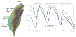
Map Templates from https://landslide.geologycloud.tw/
Reservoir data source: https://water.taiwanstat.com
The Taiwanese government has taken many measures to address the water shortage problem, including transferring water between reservoirs, stopping water supply for agriculture, reducing water supply for households, drilling groundwater wells, and desalinating seawater. Besides, industrial users, including semiconductor manufacturers, have been asked to reduce their water consumption. TSMC, for example, has significantly increased the water recycling rate. The water level in the northern reservoirs has reached a multi-year low, though still sufficient for the continued use by Hsinchu Science Park (HSP). However, the average effective water storage of the reservoirs supplying the Central Taiwan Science Park (CTSP) and Southern Taiwan Science Park (STSP) on April 30 was only 8.9% and 14.3% respectively (Exhibit 2). According to Counterpoint estimates, if there is no heavy rainfall or the rainfall does not fall in the catchment area, CTSP will face a water outage in July and STSP around August. Given that the current capacity utilization rate of most semiconductor fabs is close to 100%, this is bound to worsen the ongoing semiconductor shortage. Semiconductor manufacturing vendors should (1) consider relocating their production to other regions to mitigate the impact and (2) prioritize the production sequence to avoid a disconnected electronic supply chain.
The post Taiwan Drought May Worsen Global Component Shortage appeared first on Counterpoint.
]]>The post Smartphone Storage Capacity Zooms on Increased Demand appeared first on Counterpoint.
]]>The global smartphone industry is experiencing an increasing trend of adoption of larger NAND capacities. In 2020, smartphones crossed the 100GB mark for average NAND capacity. The high-end smartphones benefitted from the high-capacity and high-speed UFS NAND, whose prices reduced significantly in the past two years, according to our Component Price Tracker.
With their higher price point, iPhones have historically retained a much higher average NAND-flash density compared to their Android peers. However, this gap is quickly reducing due to (i) Apple’s decision to limit the iPhone 12 storage to 512GB and (ii) rapidly rising storage capacities in Android smartphones as per our historical data and forecast of smartphone memory for the 2018-2024 period.
NAND capacity ranking of smartphone OEM brands
Huawei led the average NAND flash content rankings in Q4 2020. As shown in the chart below, Huawei was closely followed by Apple and OPPO while Motorola and LG found themselves at the list’s bottom. Here, the top players shipped phones with average NAND capacities of over two times that of the players at the bottom of the list.

Huawei’s average NAND density was much higher than any other Android OEM in Q4 2020, reflecting its focus on the high-end smartphone segment in the past few years to improve margins. In the 2019-2020 period, nearly half of Huawei’s and Apple’s smartphone shipments came from their 128GB and 64GB variants, respectively. In the same period, Huawei’s and Apple’s 128GB variants experienced a yearly growth in low-to-mid teens for shipments. In comparison, their 64GB variants saw nearly a double-digit and over 1% decline, respectively.
According to our Global Handset Model Sales Tracker, the Huawei P30, P30 Lite and P30 Pro collectively made up for nearly one-eighth of the company’s 2019-2020 shipments. From these, the 128GB variants accounted for roughly three-fourths of the sales. The company’s top 20 shipped model families made up over half of its sales. Out of these, the 128GB variants made up nearly 60% of the shipments.
On the other hand, the iPhone 11, iPhone XR and iPhone 11 Pro Max together accounted for nearly half of Apple’s shipments in the 2019-2020 period. Among these model families, the 64GB variants made up for over half of their sales. OPPO’s top five best-selling smartphones contributed to 30% of its 2019-2020 shipments. Among them, the 32GB, 64GB and 128GB variants took nearly one-third of the shipments each.
Smartphone shipments dominated by 128GB NAND
For smartphone NAND Flash, 128GB is becoming the minimum standard for storage capacities in the mid-end to high-end segment. According to our Smartphone NAND Flash Status Update for Q4 2020, over one-fifth of the sub-64GB smartphone market jumped to 128GB. A similar but smaller transition occurred from 64GB to 256GB-plus variants. As a result, the 64GB-plus market experienced dramatic growth driven by (i) rising consumer demand for high-resolution video content and games, and (ii) significant price drop in eMMC and UFS NAND flash in the past few years.
Conclusion
Falling prices of high-speed UFS/uMCP storage and the inclination of smartphone users towards more extensive storage capacities have gone hand in hand to raise the market share of 64GB-plus smartphones in 2019-2020.
A detailed report on ‘Smartphones Memory Historical Data and Forecast, Worldwide Demand, 2018-2024’ is available on our website for paying subscribers.
Authors:
Related Posts
- Average Smartphone NAND Flash Capacity Crossed 100GB in 2020
- How 5G, AI and IoT are Shaping Future of Storage
- Storage Capacity Requirement for Autonomous Vehicles in the Next Decade
- Three Improvements Apple Made for Cameras of its iPhone 12 Pros
- Apple Silicon Set to Energize PC Market as Possibilities Beckon
- Apple ‘Arms’ Macs with Apple Silicon
The post Smartphone Storage Capacity Zooms on Increased Demand appeared first on Counterpoint.
]]>The post Average Smartphone NAND Flash Capacity Crossed 100GB in 2020 appeared first on Counterpoint.
]]>According to Counterpoint’s latest report on smartphone memory, the average smartphone NAND flash capacity crossed the 100GB mark in 2020 for the first time. However, it differs in iOS and Android phones. In iOS phones, the average NAND capacity reached 140.9GB in Q4 2020, compared to 95.7GB in Android phones during the same period. But this gap is narrowing. It is evident from the graph below that the average capacity of Android has been increasing rapidly in the past few years. The average capacity in 2020 grew 5.6% and 20.5% for iOS and Android phones, respectively.
Exhibit 1: Global Average Smartphone NAND Flash Capacity by iOS and Android
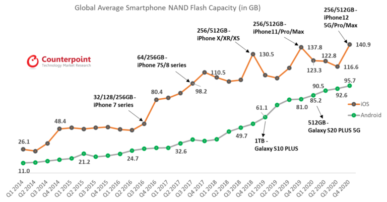
The data indicates that Apple did not push the boundaries of its storage size and chose to stick to 512GB NAND, its highest storage capacity which has been there since 2018. On the other hand, the biggest Android OEM, Samsung, looked to maximize its storage capacity and launched the Samsung Galaxy S10 Plus in 2019 with 1TB NAND. All this resulted in a lower storage growth rate for iOS compared to Android in 2020.
According to our Q1 2019-Q4 2020 mobile handset sell-through tracker, NAND flash in smartphones grew by 20.3% on average, from 80.7GB in 2019 to 97.11GB in 2020. However, iOS saw a 5.6% increase in 2020, much lower than the 20.5% growth in non-iOS devices. The difference in average capacity between iOS and non-iOS devices continues to decrease. The gap between the two groups was approximately 45.2GB in Q4 2020, down from 56.8GB in Q4 2019.
Although NAND price continued to fall during 2019-2020, the share of sales of high-capacity models (256GB and 512GB) for iOS did not grow during the same period. The share of high capacity in Q4 2020 was about 21.5%, even lower than the 27.2% in Q4 2019. The average capacity of iOS has reached nearly 130GB. 128-256GB is high enough for the average consumer to use during the iPhone usage cycle. The demand for 512GB iPhone was around 3.7% in Q4 2020.
We also observe a similar situation for high capacity (256GB+512GB+1,024GB) in non-iOS smartphones. The proportion of high capacity was around 7.5% in Q4 2020, only slightly higher than the 6.3% in Q4 2019. However, the proportion of 128GB for non-iOS smartphones increased from 26.2% in Q4 2019 to 39.0% in Q4 2020, showing that 128GB was the minimum standard for mid-range and high-end phones.
For the details, please check the report on our website.
Smartphones Memory Historical data and Forecast, Worldwide Demand, 2018-2024
Overview:
This forecast provides detailed statistical data for DRAM and NAND flash for smartphones by density, segment and network in the short and long terms.
Table of Contents:
- Historical NAND Flash Units Sell-through by Smartphone Segment (Q1 2019 – Q4 2020)
- Historical NAND Flash Units Sell-through by Smartphone Network (5G, 4G, Others)
- Historical NAND Flash Units Sell-through by Smartphone Density
- Historical NAND Flash Units Sell-through by Smartphone Density
- Forecast Memory Units Shipment in Annual Base (2018-2024)
- Charts
- Global average smartphone NAND flash capacity trends (GBs), 2014-2020
Author: Brady Wang
Number of Pages: 33
Published Date: March 2021
Related Posts
- How 5G, AI and IoT are Shaping Future of Storage
- Storage Capacity Requirement for Autonomous Vehicles in the Next Decade
- Three Improvements Apple Made for Cameras of its iPhone 12 Pros
- Apple Silicon Set to Energize PC Market as Possibilities Beckon
- Apple ‘Arms’ Macs with Apple Silicon
- Rising UFS Shipments Opens Up Opportunity for Western Digital and Toshiba Memory Corporation
The post Average Smartphone NAND Flash Capacity Crossed 100GB in 2020 appeared first on Counterpoint.
]]>The post Semiconductor Component Shortage Hits Automobile Industry appeared first on Counterpoint.
]]>COVID-19 reduced automobile sales in H1 2020. The demand started recovering in H2 2020 in many regions but here, too, the pandemic proved to be a spoiler by impacting automotive electronic manufacturing. Furthermore, the limited capacity expansion of 8-inch semiconductor production in the past few years has intensified the shortage. In the short term, this has led to price increases. In the long term, this will transform the global automotive electronics ecosystem.
Automotive electronics’ quality requirement may be rigid and qualification process complicated, but the profit margins are stable and high. Besides, since its product lifecycle is long, it is always the target market for most semiconductor suppliers.
Outsourcing of production to foundry partners
The investment required for setting up an in-house advanced semiconductor manufacturing facility is not only huge but also risky. Further, the reliability testing, verification and qualification of automotive semiconductors may take a long time, affecting the short-term and long-term utilization rates of production plants. Also, both frontend and backend processes need to be optimally synchronized to develop competitive and high-quality products.
As a result, most automotive IDMs (Integrated Device Manufactures) have not set up any new fabs in the past three years and continue to increase the proportion of outsourced manufacturing to reduce production risk. For example, Infineon has decided to increase the foundry service percentage to 70% and 25% for logic and power components, respectively. Renesas has been reducing its fab capacity since 2011 and adding orders to TSMC to become a fab-lite IDM.
The top five automotive electronics companies – NXP, Infineon, Renesas, Texas Instruments and STMicroelectronics – were all affected by COVID-19 in H1 2020. The most affected semiconductor components were microcontrollers (MCUs) and power semiconductors.
Exhibit 1 Automotive Semiconductor Supply Chain
MCU
The major suppliers of automotive MCUs include Infineon, STMicro and NXP. Due to the impact of COVID-19 in Europe, the capacity utilization of these IDMs has not recovered. For example, STM’s capacity utilization is only 70%-80%. The most significant impact of the MCU shortage is on the Electronic Stability Program (ESP), also known as Electronic Stability Control (ESC), which is an essential part of the vehicle computer. In the fourth quarter, MCU delivery time for ESP products has been extended and prices increased.
In response to the growing demand for wireless connectivity, smart and electric vehicles, most of these companies outsource their MCU production to other foundries using 28nm and below technologies. NXP’s technology in its fab is only 90nm, so it has to outsource most of its high-end production MCUs. NXP has also established a factory in Singapore with TSMC. However, TSMC and UMC are currently running at full capacity in almost all production lines. UMC has announced that it would increase the prices for its 8-inch products. Therefore, the MCU prices will continue to increase while the delivery time will get extended.
Power semiconductors
The demand for power semiconductors in the automotive industry continues to rise with the soaring electronic content in vehicles. The market for power semiconductors is expected to grow even further as ADAS (Advanced Driver Assistance Systems), electric and hybrid cars become more prevalent.
Power semiconductor devices are the core devices for power conversion, accounting for about 50% of the automotive semiconductor market. Their primary applications include inverters, voltage converters and gate drivers used to supply and regulate power systems.
IDMs’ in-house production facilities still dominate today’s power semiconductor production. However, outsourcing is increasing, especially for regular products. For example, Infineon is building a 12-inch power semiconductor factory while increasing outsourcing, which is expected to reach 15% in the next four years.
Short-term trends
- Automotive semiconductor shortages may decrease automobile production in Q1 2021, especially in major car producing countries such as China and India, as the main supply of their automotive semiconductors comes from Europe, North America and South Asia, where production has slowed down due to COVID-19. At present, 88.5% of China’s automotive semiconductor MCUs are from other countries, and this number is even higher for India.
- Usually, car manufacturing follows the JIT (just in time) inventory management system that allows the carmakers to keep low inventory. However, in an uncertain situation, every stakeholder in the ecosystem will try to increase inventory, thus worsening the component shortage.
Long-term trends
- Automotive semiconductor production will increase to meet the growing market, either by expanding or migrating from the 8-inch to 12-inch fabs.
- The increasing electronic content in vehicles will motivate major auto-producing countries to increase local production.
Conclusion
In the short term, the supply shortage of automotive semiconductors will continue till Q3 2021, but the price increase will continue till 2022.
The post Semiconductor Component Shortage Hits Automobile Industry appeared first on Counterpoint.
]]>The post Apple Silicon Set to Energize PC Market as Possibilities Beckon appeared first on Counterpoint.
]]>Just like iOS and Android, Apple’s macOS has a different ecosystem than Windows. Although macOS has continued to improve its user interface, Apple’s service revenue from the PC segment can’t be compared with that from the iPhone. The slow improvement in PC hardware, which is dominated by Intel, is among the key factors affecting macOS’ progress. The gap between the two operating systems is also getting smaller as Windows is catching up. On the other hand, thanks to the healthy competition between the two major smartphone operating systems, smartphones have improved system architecture, such as memory management, power management, artificial intelligence functions, and user interface. They have integrated new chips, such as UWB, GPS and LIDAR, to meet the AI and IoT demand. The OS is undoubtedly the critical determinant of system performance. However, the most vital remains the brain — microprocessor.
Intel dominated the entire PC architecture for several decades. Many peripheral connections (such as wired and wireless connectivity), memory configurations, and integrated GPU and AI chips remained constrained by the Intel architecture. As a result, PCs and NB ODM/OEMs saw limited innovation. They just (or could only) followed Intel’s roadmap for x86 architecture advances. x86 has not been able to create many innovative applications to fulfill the emerging requirement for AI and IoT.
To overcome this, Apple announced at this year’s Worldwide Developers Conference (WWDC) that its entire Mac product line would switch from Intel chips to Apple Silicon within two years, and officially released the Apple M1 on November 10.
The M1 specifications are similar to those of the A14 Bionic. However, the M1 on a Mac device can deliver more computing power and applications than the A14 Bionic on an iPhone. Both are manufactured at TSMC’s 5nm and feature custom high-performance (Firestorm), energy-efficient (Icestorm), GPU and NPU. However, the M1 has two more high-performance cores than the A14 Bionic, as well as additional cache and peripheral circuitry.
The purpose of the first generation of Apple Silicon, M1, is to create a new experience. It aims to achieve the balance of performance and power consumption, instead of high computing. According to Apple, the M1 has 16 billion transistors, about 35% more than the A14 Bionic. Counterpoint estimates that the M1 die size is approximately 140-150mm2, much larger than that of the A14 Bionic.
Depending on the applications’ environment, power consumption, thermal efficiency and footprint are essential considerations in designing SoCs. Thanks to the advantages of the advanced process in TSMC in terms of power consumption and transistor density, the M1 performs better on Mac devices than on previous Intel-based MacBook. Unlike Intel CPUs that emphasize a maximum clock rate, the Apple M1 clock rate is dynamic. The M1 utilizes energy-efficient cores to achieve lower system power consumption and multitasking workload. However, in addition to the limitations inherited from the Apple AX SOC, the M1’s maximum clock rate cannot boost to 4.8GHz like Intel’s latest Tiger Lake CPU (10nm), which is more likely due to TSMC’s process limitations.
It is worth mentioning that the M1 embeds DRAM next to the SoC to form a unified memory architecture (UMA) to speed up data access through high-speed inter-connections. In contrast to the A14 Bionic, the DRAM is placed next to the SOC instead of being stacked. This idea has been mentioned in many documents, but its use in a PC is groundbreaking. As Michael Dell once said, “Ideas are commodities, execution is not.” Apple has managed to prove the benefits of UMA through actual product design and validation.
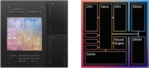
Source: Apple
Below are the advantages of this packaging method:
- The embedded DRAM in the M1 can reduce memory modules’ footprint, leaving room for batteries or other peripheral circuits.
- The signal transmission speed between the SOC and DRAM in the same package is much faster than in the design where the chip is separated at different positions on the PCB. Of course, it becomes more difficult to manufacture such chips. But TSMC’s advanced packaging technology enables such a design.
- Unlike the legacy architecture in traditional PCs, the M1 embeds high-bandwidth and low-latency memory DRAM into a single pool within a custom package. Therefore, all cores can retrieve data in the memory simultaneously, and the system can dynamically arrange the precious memory resource. This dramatically improves system performance and reduces the usage of power-hungry DRAM, consequently extending the battery life.
As we mentioned in a report published in June, the benefits of migrating to the new architecture (Apple Silicon) include:
- Reducing reliance on a single supplier
- Differentiating products from competitors
- Gaining control of the ecosystem
- Developing apps for both mobile and computer using the same APIs and programming tools.
- Reducing cost
The usage of the M1 in Mac devices demonstrates these benefits. In terms of cost reduction, the M1’s production cost is lower than the Intel CPU’s purchase cost. Therefore, the overall price of the system will be lower than before.
Further possibilities with Apple Silicon include:
- Multi-cores: The next generation of Apple chips will have more high-performance cores to meet the requirements of multitasking and high-performance PC applications. However, this will inevitably be accompanied by an equivalent increase in embedded SRAM density, leading to a significant cost increase. Therefore, if the technology migration becomes slower, dual Apple Silicon coexistence may be a potential solution.
- Powerful NPU: The NPU allows the Mac devices to enhance AI inferring capabilities in image and voice, such as integrating virtual assistant (macOS Siri) to enhance the Mac’s strengths in the office, reducing the bandwidth required for remote video-conferencing and providing instant translation at the edge.
- Integrated discrete GPU chips: Thanks to its high-performance GPU core driven by TSMC 5nm, the M1 is more powerful than the mid-range standalone GPU graphics cards. However, it is still insufficient for content creators. Therefore, Counterpoint believes Apple Silicon will integrate AP and GPU into a single chip by using advanced package
(To be continued. This is Part I of a series)
Related Posts
- Apple ‘Arms’ Macs with Apple Silicon
- iOS 14 to macOS Big Sur and Apple Silicon, Top Announcements from WWDC 2020
- Seemingly Hasty, but Prudent TSMC’s New Fab Plan in the U.S.
The post Apple Silicon Set to Energize PC Market as Possibilities Beckon appeared first on Counterpoint.
]]>The post NVIDIA-Arm deal, if successful, will bring dramatic changes to industry appeared first on Counterpoint.
]]>Since both NVIDIA and Arm are leading vendors in their own territories, the complementary synergies between the two are expected to make the deal a win-win for both. At the same time, the deal will create more concern for other stakeholders.
Arm is a company that almost monopolizes the SoC core design in several segments. However, Arm is not involved in chip manufacturing or creates any chip with its own brand. Instead, it licenses IP, instruction set architecture (ISA) and other technologies to other chip companies, allowing them to design their own unique SoCs for a variety of applications. In the past, the low power consumption capability of Arm’s IP allowed it to grow and dominate in the mobile device market. Currently, almost all mobile phones, tablets and IoT devices use Arm technology. In recent years, it has gradually expanded to high-speed computing devices such as PCs, and data centers.
NVIDIA specializes in graphics processing technology and is one of the leading GPU vendors. Thanks to the fast-growing demand for AI and high performance of its GPU, Nvidia has become one of the leading vendors both in edge computing and data center in the past few years.
While NVIDIA and Arm have quite complementary businesses, they also share common goals, such as the server and data center businesses. By combining Nvidia’s AI capability and Arm’s complete ecosystem for edge devices, NVIDIA hopes to empower more edge devices, including smartphones, PCs, self-driving cars, robots and 5G devices, to be able to process inference.
- From the perspective of the server market, Arm plans to launch a series of Neoverse microarchitectures in an attempt to expand its service beyond the mobile device. However, Arm’s progress in the server segment remains slow because of its weakness in AI. Therefore, the acquisition by NVIDIA will accelerate the use of Arm chips in data center.
- From the perspective of the computer market, Arm recently introduced the Cortex X1 CPU core, which is designed for flagship smartphones and other high-performance mobile devices. It is expected that NVIDIA will support Arm to design powerful cores for x86 platforms. However, this is something that some of the competitors will not like. A new Arm core with higher computing power will also shorten the gap with existing x86 CPU vendors.
- From the perspective of the mobile phone market, NVIDIA is unlikely to launch its own smartphone APs. NVIDIA believes that it is a software company. Therefore, licensing could be more in line with its current direction. Just as Arm’s licensing business, NVIDIA could license its GPU and AI cores to other SoC vendors, along with other Arm CPU cores. This will enhance the image processing and AI capabilities of Android phones and shorten the gap with Apple’s SoC. Also, this will enhance the competitiveness of Arm’s IP.
The AIoT market is undoubtedly the initial target of NVIDIA-Arm merger, but the data center is the final. NVIDIA’s AI started in the cloud and is moving quickly to the edge, such as warehouses, hospitals, streets and airports. With the deployment of AI capability moving from the cloud to edge, smart sensors connected to AI computers can improve the user experience and save cost. These small autonomous machines will compute continuously and connect to powerful cloud data centers in every corner of the world.
However, NVIDIA’s merger with Arm may run into hurdles, such as opposition from other related companies and antitrust examination in different regions.
- Arm’s existing partners may switch to RISC-V, which is a new free and open-source architecture, if they feel that Arm’s integrity and independence are being compromised. Counterpoint believes that although the RISC-V Foundation already has many important players and RISC-V is already being used to design MCU, the gap between it and Arm is still quite large and will take time to build comprehensive ecosystem. Therefore, it is almost impossible to replace Arm on mobile phones in the next five years. In addition, RISC-V will still face the same problem as Arm — how to remain in a neutral position while keeping business growth.
- According to NVIDIA, the proposed transaction is subject to customary closing conditions, including the receipt of regulatory approvals from the US, UK, China and the European Union. The transaction is expected to be completed in around 18 months. The uncertainties of this deal mostly stem from the current trade dispute between the US and China. As the deal will change the jurisdiction of Arm, from the UK and Japan to the US, the Chinese approval to the transaction becomes important. In addition, Arm is still locked in a dispute over the control of its Chinese subsidiary. Counterpoint believes NVIDIA will need to have more communication as well as guarantees and concessions to resolve the issue. The good news is that NVIDIA has a lot of investment and partners in China, making it easier to get approvals.
Conclusion
Through this acquisition, NVIDIA wants to enhance the AI capabilities of Arm-based IoT endpoints to achieve smart devices everywhere, while continuing to consolidate its position in the data center segment. However, the acquisition is still challenging and unpredictable and may take longer than expected to produce the desired result.
The post NVIDIA-Arm deal, if successful, will bring dramatic changes to industry appeared first on Counterpoint.
]]>The post Huawei’s Travails may Bring 5G Windfall for MediaTek appeared first on Counterpoint.
]]>Takeaways from the earnings call include:
- Global 5G smartphone shipments will reach 170 million to 200 million units in 2020 while China will reach 100 million to 120 million units. The total volume will be more than double in 2021.
- MTK believes its share in the 5G SoC market in volume terms will be above 40% in China and more than 20% globally by the end of 2020.
- Major Chinese smartphone brands are shipping 5G smartphones equipped with MediaTek. There are also other competitive MTK models preparing to launch in 2020.
MediaTek’s estimates for 2020 5G smartphone shipments are close to Qualcomm’s. Qualcomm estimated in its June earnings call that global 5G smartphone shipments in 2020 would be between 175 million and 225 million, compared to MediaTek estimate of between 170 million and 200 million.
Qualcomm and MediaTek are targeting slightly different price ranges for smartphones. According to Counterpoint data, in the second quarter, most smartphones with MediaTek SoCs were priced at $150-$399 (Dimensity 800) and $250-$499 (Dimensity 1000) while smartphones with Qualcomm SoCs were priced at $400-$799 (Snapdragon 865).
Like Qualcomm, MediaTek is very confident of its 5G sales in China, believing that all major Chinese mobile phone brands have adopted its 5G SoC products. Thanks to the strong demand and promotion of 5G smartphones and services in China, MediaTek expects its China 5G market share to reach 40% by the end of 2020. However, Counterpoint’s monthly smartphone sales tracker shows MTK chips accounted for only 7.6% of China’s 5G SoCs in May. On the other hand, Huawei (HiSilicon) has a 63% market share of 5G SoCs in China due to Huawei’s strong growth in the second quarter.
Under a ban announced by the US Bureau of Industry and Security (BIS) on May 15, Huawei will not be able to get any product made for it at its most important foundries (TSMC’s) 120 days after the effective date, which is September 15. This makes Huawei unable to use its Kirin SoC. Furthermore, Huawei’s options are limited, and the ban forces it to use SoCs from competitors. Therefore, if the share of MediaTek’s SoC reaches 40% of China’s 5G market by the end of 2020, it is bound to see MediaTek’s 5G chips being widely adopted by Huawei. Besides, since Huawei’s cutting-edge SoC was being produced at TSMC’s 5nm, the switch to MTK SoC will also affect TSMC’s capacity allocation.
Therefore, under the two assumptions of (1) Market shares of all smartphone OEMs in China remaining unchanged and (2) Sell-through of 5G smartphones in China in 2020 reaching 100 million and MediaTek’s 5G SoC share reaching 40% in Q4 2020, Counterpoint’s estimates of MediaTek’s 5G chip shipments and its share of TSMC’s 7nm capacity in the third quarter are as follows:
- Demand for MTK’s 5G chips is expected to increase by 218.6% compared to the period before the announcement of US BIS ban.
- Assuming a 90% yield rate (7nm) and a GDPW (gross die per wafer) average of 645, this will account for 12.6% of TSMC’s Q3 7nm production capacity.
Exhibit: Share of 5G chipsets in China, 2020
Conclusions and Recommendations
- Huawei (HiSilicon) will slowly lose its strengths in chip design because now it cannot work with TSMC to develop new processes.
- Due to the use of third-party chips, the overall cost of Huawei’s premium smartphones will increase, reducing their attractiveness.
- In the next few years, the securing of TSMC’s cutting-edge capacity will remain most critical for smartphone SoC. However, in future, Huawei will not be able to secure capacity directly with TSMC and will have to do so indirectly through its SoC suppliers.
- Like Apple, Huawei has used its in-house chip design company in the past to get the most out of its smartphones. However, in future, Huawei will have to put more effort into differentiating itself (like HMS) to outperform other smartphone OEMs that use MTK SoCs as well.
- Reliance on a single supplier will make Huawei’s smartphone plans (such as production and roadmaps) more accessible to competitors. Huawei should source its APs from multiple suppliers to reduce the reliance and increase pricing power.
Related Posts
- One in Three Smartphones Sold was a 5G Phone in China in Q2 2020
- TSMC Caught in the Crossfire as US Renews Focus on Huawei
- Apple ‘Arms’ Macs with Apple Silicon
The post Huawei’s Travails may Bring 5G Windfall for MediaTek appeared first on Counterpoint.
]]>The post Apple 'Arms' Macs with Apple Silicon appeared first on Counterpoint.
]]>Analysis
The benefits of migrating to the new architecture (Apple Silicon):
- Reducing reliance on a single supplier
- Differentiating products from competitors
- Gaining control of the ecosystem
- Allowing developers to develop apps for both mobile and computer applications using the same APIs and programming tools.
- Reducing cost
Cost reduction is one of Apple Silicon’s advantages over Intel CPUs because the former will be produced with TSMC‘s advanced technology. In the past few years, Intel has been struggling to improve its chip manufacturing process, which has stayed at 14nm/10nm, falling behind TSMC’s 5nm in 2020. This gives Apple a motivation for the migration and a belief that the performance of its self-designed chips can be better. However, although cost reduction is one of Apple Silicon’s most important advantages, we believe that this is not the main purpose of Apple’s architecture change. The main aim here seems to be to increase service revenue. Apple expects to replicate the success of iPhone/iPad in its PC business. The company’s services business generated $2.7 billion in revenue in 2019, far exceeding Google’s Android. Also, its service revenue has surpassed that from Mac since 2016, accounting for 18% in 2019.
Apple’s revenue breakdown from 2007 to 2019
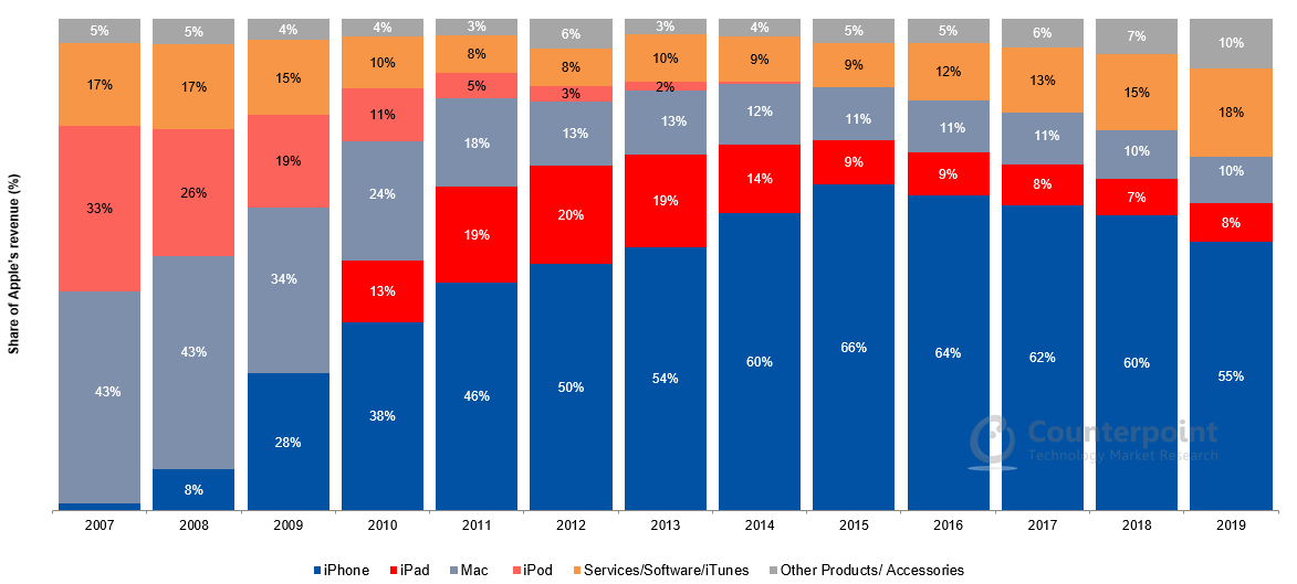
Apple’s self-designed chips include not only ARM compatible cores but also non-ARM cores for GPU, camera fusion, audio/video processors, accelerator, memory controller, neural processing unit (NPU), and others. The non-ARM cores take even larger space than ARM cores in SoC. The integration of these cores in a single SoC results in significant cost savings and provides additional features. These investments are expensive but provide solid and differentiated functionalities that are difficult for competitors to deal with. Apple will continue to extend this advantage to its future chips for Macs. To help apps migration, Apple will design special functions to help emulators build into new Mac OS running old Intel apps on the new platform. In addition, Apple will be able to use its neural engine to speed up non-linear video editing software and apps for machine learning and AI.
Future Apple Silicons
Although the developer transition kit uses a modified Mac mini with an A12Z chip that has been used in iPad Pro, we believe Apple is unlikely to merely reuse existing chips for iPhone or iPad in Macs. There could be two lines of Mac-specific SoC processors for different markets – one for light laptops such as Macbook Air, Macbook Pro and possibly iPad Pro, and the other for ultra-high-performance desktop Macs such as iMac Pro and Mac Pro. The primary goal of a laptop-grade SoC would be to have balance between performance and power consumption. The highly integrated PCB and the laptop-grade SoC, which is smaller than Intel’s CPU, can reserve more space for battery packs. Conversely, in situations where battery life and chip size are not major concerns (like in a desktop Mac), the performance of the chip can be maximized. The initial production linewidth of Apple Silicon will be 5nm and stay at that level for two to three years since Apple and TSMC need to cooperate to improve the performance of the new chips.
Future Macs
- PCB components will be more compact in future laptop Macs, including MacBook Air and MacBook Pro. This will allow the new Macs to use the up-to-date high-performance processors and other components in a smaller package, leaving more room for battery packs.
- New Macs may adopt BGA-SSD or even raw NAND that will be managed directly by Apple Silicon. This can save some space and costs of controllers.
- Since the ARM core will consume less power, it will not require a large fan as in Intel-based Macs. The saved space will be used for the battery as well.
- The functions of Macbook Air and iPad Pro will become very close. The former is like a clamshell laptop and the latter is like a detachable laptop.
- Future Macs are expected to integrate more sensors, such as 3D sensing and ultra-wideband (UWB). The SoC here will incorporate more powerful NPUs to process the image captured by iPhone 12 and iPad Pro.
- Although the cost of Apple Silicon is lower than Intel’s CPU, the price of future Macs will not necessarily be cheaper than the current models. On the other hand, the price may increase because of the new design with additional sensors and chips.
Companies Involved
- TSMC: 5nm will be the mainstream technology of Apple Silicon in the next two to three years. In addition to Apple, it is expected to see other SoC vendors working on ARM-based SoC for PC, which will become the next battlefield in the foundry industry.
- ARM: ARM will benefit from the license fee that Apple will pay to migrate its platform.
- Intel: Intel will suffer revenue loss from the transition. However, its impact will be limited. Intel is expected to move to 10nm/7nm soon to stop the increasing adoption of ARM-based SoC in PC.
Related Posts
- iOS 14 to macOS Big Sur and Apple Silicon, Top Announcements from WWDC 2020
- TSMC Caught in the Crossfire as US Renews Focus on HuaweiTSMC Caught in the Crossfire as US Renews Focus on Huawei
- Seemingly Hasty, but Prudent TSMC’s New Fab Plan in the U.S.
The post Apple 'Arms' Macs with Apple Silicon appeared first on Counterpoint.
]]>The post The NAND flash consumption of mobile devices will be three times larger in 2025 than 2021, with the coming of the 5G era appeared first on Counterpoint.
]]>5G adds complexity as each mobile device to both generate, as well as consume, several times more data than current devices. Higher 5G throughputs will drive richer content streaming. More advanced AI applications will add further complexity to the choice of storage. Considering storage early in the design phase will help to improve the performance of 5G mobile devices and will potentially be a point of differentiation among competing products.
The key trends for storage in 5G-capable mobile devices:
- Better performance in sequential reading/writing speed and bandwidth
- Larger capacity to 256GB, 512GB, and above
- Lower costs including 3D NAND, TLC, QLC
- Better controller qualities in architecture, lifetime, wear leveling, over-provisioning
- Embedded Storage Interfaces including UFS 2.1, UFS 3.x, UFS4.x, and PCIe
- Better reliability to improve the lifetime of the device
The key mobile devices to be driven by 5G include smartphones, connected PCs, tablets, and standalone eXtended Reality (XR) head-mounted-displays (HMD). All these devices will have different requirements for storage. Many of these devices will also drive new use cases, potentially generating more service revenue as outlined in the diagram:
![]()
Opportunity for storage players
eMMC 5.1 can still meet the demand for some devices migrating initially from 4G to 5G. However, The UFS interface aligns best with most 5G devices because of its high Gbps-level throughputs. Connected PCs will need both UFS storage and PCIe SSDs, while others will prefer UFS as the main storage interface.
From the perspective of the package, MCP solutions are dominant only in the low to mid-range smartphones. While system designers for high-performance mobile devices prefer to use package-on-package (PoP) solution which includes low power DRAM plus discrete UFS or eMMC. PoP solutions can provide better performance than MCP solutions because the application processor (AP) can directly communicate with low power DRAM at high frequencies to reduce the interference of AP and RAM communication signals.
![]()
From the perspective of performance, eMMC has become the mainstream of mobile application data storage for several years. However, the speed of eMMC is reaching a limit because of its parallel 8-bit transmission. As a result, UFS is poised to become the mainstream interface in the 5G era because its serial interface and full-duplex data transfer protocol can offer two to four times the peak bandwidth of eMMC’s parallel 8-bit interface. UFS 2.x and UFS 3.x can reach a maximum speed of 11.6Gbps (1450 MB/s) and 23.2Gbps (2,900 MB/s), respectively. Both are much higher than eMMC 5.1’s 3.2Gbps (400 MB/s). Future UFS 4.x can be even faster.
![]()
The UFS interface aligns well with the higher Gbps level throughputs promised in 5G, compared to eMMC which could be a bottleneck for some 5G-driven mobile devices such as connected PCs, XR devices, smartphones, and tablets. Further, the power consumption of UFS in standby mode is like that of eMMC. In the active mode, UFS power consumption is higher than eMMC but UFS can rapidly transmit more data, allowing a return to an idle state faster. So, UFS is significantly lower compared to eMMC in terms of overall power consumption and can enable battery savings for battery-powered IoT applications. Further, UFS also delivers greater overall system performance and user experiences, which makes it the choice of memory storage interface for 5G mobile devices.
Compared to 5G’s 1-10 Gbps, the theoretical transmission rate of 4G LTE can exceed 1Gbps, but the actual speeds in most cases are still below 500Mbps. 5G-powered XR, online game, and 8K video will require speeds of 6 Gbps, so UFS is essential in these applications.
![]()
Conclusion & Recommendations
- UFS is the most suitable interface for 5G-driven mobile devices. Its fast speed and responsiveness can meet the requirements of instant-on, fast-booting, multitasking, and multiprocessing in the 5G era. Also, it consumes less power so it can extend battery life.
- Mobile game streaming will grow strongly with 5G’s large bandwidth and low latency. Content providers need to know the capability, requirements, and limitations of 5G and design high-quality mobile games with cloud streaming on any device.
- The price of NAND flash is declining. However, 5G-centric devices will require high-performance storage solutions. Mobile devices manufacturers must understand the characteristics of different types of flash to choose the appropriate memory to meet the performance requirements of their applications.
- To be successful in the 5G era, flash makers must understand the demand and the impact of these 5G devices on storage and realize the market potential for various applications to provide the right solutions
Download the Whitepaper: The NAND flash consumption of mobile devices will see three times larger in 2025 than 2021, with the coming of the 5G era. (for free)
The post The NAND flash consumption of mobile devices will be three times larger in 2025 than 2021, with the coming of the 5G era appeared first on Counterpoint.
]]>